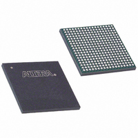
EPM2210F324C3 Altera, EPM2210F324C3 Datasheet - Page 54

EPM2210F324C3
Manufacturer Part Number
EPM2210F324C3
Description
IC MAX II CPLD 2210 LE 324-FBGA
Manufacturer
Altera
Series
MAX® IIr
Specifications of EPM2210F324C3
Programmable Type
In System Programmable
Delay Time Tpd(1) Max
7.0ns
Voltage Supply - Internal
2.5V, 3.3V
Number Of Logic Elements/blocks
2210
Number Of Macrocells
1700
Number Of I /o
272
Operating Temperature
0°C ~ 85°C
Mounting Type
Surface Mount
Package / Case
324-FBGA
Voltage
2.5V, 3.3V
Memory Type
FLASH
Number Of Logic Elements/cells
2210
For Use With
P0305 - KIT MAX II MICRO
Lead Free Status / RoHS Status
Contains lead / RoHS non-compliant
Features
-
Other names
544-1344
EPM2210F324C3
EPM2210F324C3
Available stocks
Company
Part Number
Manufacturer
Quantity
Price
Company:
Part Number:
EPM2210F324C3
Manufacturer:
ALTERA
Quantity:
784
Company:
Part Number:
EPM2210F324C3N
Manufacturer:
ALTERA
Quantity:
852
4–4
Figure 4–2. Transistor-Level Diagram of MAX II Device I/O Buffers
Figure 4–3. ESD Protection During Positive Voltage Zap
MAX II Device Handbook
n+
The CMOS output drivers in the I/O pins intrinsically provide electrostatic discharge
(ESD) protection. There are two cases to consider for ESD voltage strikes: positive
voltage zap and negative voltage zap.
A positive ESD voltage zap occurs when a positive voltage is present on an I/O pin
due to an ESD charge event. This can cause the N+ (Drain)/ P-Substrate junction of
the N-channel drain to break down and the N+ (Drain)/P-Substrate/N+ (Source)
intrinsic bipolar transistor turn on to discharge ESD current from I/O pin to GND.
The dashed line (see
positive ESD zap.
IOE Signal
p - well
I/O
n+
GND
VPAD
Figure
Source
Drain
Drain
Source
PMOS
NMOS
4–3) shows the ESD current discharge path during a
Larger of VCCIO or VPAD
p+
IOE Signal or the
Gate
Gate
Chapter 4: Hot Socketing and Power-On Reset in MAX II Devices
n - well
Hot Socketing Feature Implementation in MAX II Devices
P-Substrate
VCCIO
p+
p - substrate
N+
N+
VCCIO or VPAD
The Larger of
D
S
n+
GND
I/O
G
© October 2008 Altera Corporation
Ensures 3.3-V
Tolerance and
Hot-Socket
Protection


