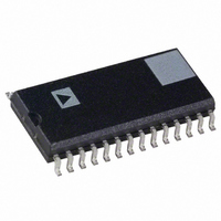
ADMCF341BR Analog Devices Inc, ADMCF341BR Datasheet - Page 17

ADMCF341BR
Manufacturer Part Number
ADMCF341BR
Description
IC DSP 3CH 12BIT MOT-CTRL 28SOIC
Manufacturer
Analog Devices Inc
Series
Motor Controlr
Type
Motor Controlr
Datasheet
1.ADMCF341BR.pdf
(36 pages)
Specifications of ADMCF341BR
Rohs Status
RoHS non-compliant
Interface
Synchronous Serial Port (SSP)
Clock Rate
20MHz
Non-volatile Memory
FLASH (12 kB), ROM (12kB)
On-chip Ram
2.5kB
Voltage - I/o
5.00V
Voltage - Core
5.00V
Operating Temperature
-40°C ~ 85°C
Mounting Type
Surface Mount
Package / Case
28-SOIC (7.5mm Width)
Available stocks
Company
Part Number
Manufacturer
Quantity
Price
Part Number:
ADMCF341BRZ
Manufacturer:
ADI/亚德诺
Quantity:
20 000
Parameter
16-BIT PWM TIMER
NOTES
1
2
ADC Overview
The ADC of the ADMC(F)341 is based upon the single slope
conversion technique. This approach offers an inherently mono-
tonic conversion process within the noise and stability of its
components, and there will be no missing codes.
The single slope technique has been adopted on the
ADMC(F)341 for four channels that are simultaneously
converted. Refer to Figure 11 for the functional schematic of
the ADC. The main inputs (I
the ADC converter through three front end blocks. Figure 15
shows the block diagram of a single front end block. Each front
end block has a bipolar current amplifier (Gain = –2.5) designed
to acquire the voltage on a current-sensing resistor whose volt-
age can be either positive or negative with respect to the power
supply ground rail.
The fourth channel has been configured with a serially con-
nected 4-to-1 multiplexer. Table VI shows the multiplexer input
selection codes. One of these auxiliary multiplexed channels is
used to acquire the internal voltage reference (V
tion purposes.
Select
VAUX0
VAUX1
VAUX2
Calibration (V
REV. B
153 Hz is calculated based on 16-bit resolution.
78,431 Hz is calculated based on 8-bit resolution.
Counter Resolution
Edge Resolution (Single Update Mode)
Edge Resolution (Double Update Mode)
Programmable Dead Time Range
Programmable Dead Time Increments
Programmable Pulse Deletion Range
Programmable Pulse Deletion Increments
PWM Frequency Range
PWMSYNC Pulse Width (T
Gate Drive Chop Frequency Range
Table VI. ADC Auxiliary Channel Selection
REF
)
MODECTRL (1)
ADCMUX1
0
0
1
1
Table V. Fundamental Characteristics of PWM Generation Unit of ADMC(F)341
SENSE1
CRST
)
to I
SENSE3
MODECTRL (0)
ADCMUX0
0
1
0
1
) are connected to
REF
) for calibra-
–17–
Single Slope ADC Operations
The ADC conversion process is done by comparing each ADC
input to a reference ramp voltage and timing the comparison of
the two signals. The actual conversion point is the time-point
intersection of the input voltage and the ramp voltage (V
shown in Figure 12. This time is converted to counts by the
12-bit ADC timer block and is stored in the ADC registers.
The ramp voltage used to perform the conversion is generated
by driving a fixed current into an off-chip capacitor, where the
capacitor voltage is:
I
I
I
SENSE1
SENSE2
SENSE3
I
VAUX0
VAUX1
VAUX2
CONST
VAUX0 (V)
VAUX1 (V)
VAUX2 (V)
VAUX3 (V)
V
VOLTAGE
VOLTAGE
VOLTAGE
CURRENT
CURRENT
CURRENT
REF
MODECTRL REG <0..1>
Min
0
153
2.0
0.02
MODECTRL REG
<09..10..11>
1
I
CONST
Figure 11. ADC Overview
REG <2:0>
CHANNEL1
CHANNEL2
CHANNEL3
MULTIPLEXER
CAPACITOR RESET
_TRIM
4-1
V
Typ
16
100
50
100
0
50
C
=
(
I C
PWMSYNC (CONVST)
I
)
CONST
COMP
COMP
COMP
COMP
×
t
Max
102
51
78,431
12.8
5
ADMC(F)341
FILTER
2
ADCAUX
V1L
V2L
V3L
VAUXL
MODECTRL
REG <07>
ADC1
ADC2
ADC3
Unit
Bits
ns
µs
ns
µs
ns
Hz
µs
MHz
ns
CLK
C
), as


