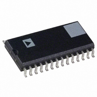
ADMCF341BR Analog Devices Inc, ADMCF341BR Datasheet - Page 21

ADMCF341BR
Manufacturer Part Number
ADMCF341BR
Description
IC DSP 3CH 12BIT MOT-CTRL 28SOIC
Manufacturer
Analog Devices Inc
Series
Motor Controlr
Type
Motor Controlr
Datasheet
1.ADMCF341BR.pdf
(36 pages)
Specifications of ADMCF341BR
Rohs Status
RoHS non-compliant
Interface
Synchronous Serial Port (SSP)
Clock Rate
20MHz
Non-volatile Memory
FLASH (12 kB), ROM (12kB)
On-chip Ram
2.5kB
Voltage - I/o
5.00V
Voltage - Core
5.00V
Operating Temperature
-40°C ~ 85°C
Mounting Type
Surface Mount
Package / Case
28-SOIC (7.5mm Width)
Available stocks
Company
Part Number
Manufacturer
Quantity
Price
Part Number:
ADMCF341BRZ
Manufacturer:
ADI/亚德诺
Quantity:
20 000
in offset mode. In offset mode, the switching frequencies of the
two signals on the AUX0 and AUX1 pins are identical and
controlled by AUXTM0 in a manner similar to that previously
described for independent mode. In addition, the on-times of
both the AUX0 and AUX1 signals are controlled by the AUXCH0
and AUXCH1 registers as before.
In this mode, however, the AUXTM1 register defines the offset
time from the rising edge of the signal on the AUX0 pin to that
on the AUX1 pin according to:
For correct operation in this mode, the value written to the
AUXTM1 register must be less than the value written to the
AUXTM0 register. Typical auxiliary PWM waveforms in offset
mode are shown in Figure 18b. Again, duty cycles from 0% to
100% are possible in this mode.
In both operating modes, the resolution of the auxiliary PWM
system is 16 bits only at the minimum switching frequency
(AUXTM0 = AUXTM1 = 65,535 in independent mode,
AUXTM0 = 65,535 in offset mode). Obviously, as the switching
frequency is increased, the resolution is reduced.
Values can be written to the auxiliary PWM registers at any
time. However, new duty cycle values written to the AUXCH0
and AUXCH1 registers only become effective at the start of
the next cycle. Writing to the AUXTM0 or AUXTM1
registers causes the internal timers to be reset to 0 and new
PWM cycles to begin. By default, following a reset, Bit 8 of
the MODECTRL register is cleared, thus enabling offset mode.
In addition, the registers AUXTM0 and AUXTM1 default to
0xFFFF, corresponding to the minimum switching frequency
and zero offset. The on-time registers AUXCH0 and AUXCH1
default to 0x0000.
Auxiliary PWM Interface, Registers, and Pins
The registers of the auxiliary PWM system are summarized in
Figure 27.
REV. B
AUX0
AUX1
Figure 18a. Typical Auxiliary PWM Signals
(All Times in Increments of t
Mode
Figure 17. Auxiliary PWM Output Filter
T
2
OFFSET
AUXCH0
AUXPWM
= ×
2
2
R1 = R2 = 13k
C1 = C2 = 10nF
AUXCH1
(
R1
AUXTM
2
C1
(AUXTM0 + 1)
R2
CK
2
1
), Independent
C2
+
(AUXTM1 + 1)
1
2
)
×
AUXCH1
t
CK
–21–
WATCHDOG TIMER
The ADMC(F)341 incorporates a watchdog timer that can
perform a full reset of the DSP and motor control peripherals
in the event of a software error. The watchdog timer is enabled
by writing a timeout value to the 16-bit WDTIMER register.
The timeout value represents the number of CLKIN cycles
required for the watchdog timer to count down to zero. When the
watchdog timer reaches zero, a full DSP core and motor control
peripheral reset is performed. In addition, Bit 1 of the
SYSSTAT register is set so that after a watchdog reset, the
ADMC(F)341 can determine that the reset was due to the
timeout of the watchdog timer and was not an external reset.
Following a watchdog reset, Bit 1 of the SYSSTAT register may
be cleared by writing zero to the WDTIMER register. This
clears the status bit but does not enable the watchdog timer.
On reset, the watchdog timer is disabled and is enabled only
when the first timeout value is written to the WDTIMER
register. To prevent the watchdog timer from timing out, the
user must write to the WDTIMER register at regular intervals
(shorter than the programmed WDTIMER period value). On
all but the first write to WDTIMER, the particular value written
to the register is unimportant, since writing to WDTIMER
simply reloads the first value written to this register.
PROGRAMMABLE DIGITAL INPUT/OUTPUT
The ADMC(F)341 has a 9-pin programmable digital input/
output (PIO) port (PORTA). The nine pins (PORTA0 to
PORTA8) are multiplexed with other on-chip peripheral
functions, in accordance with Table IX. When configured as a
PIO, each of these nine pins can act as an input or output, or an
interrupt source.
The operating mode (PIO or alternate function) of pins PORTA0
to PORTA8 is controlled by the PORTA_SELECT register.
This 9-bit register has a bit for each input so that the mode of
each pin may be selected individually.
Bit 0 of PORTA_SELECT controls the operation of the PORTA0
pin, Bit 1 controls the PORTA1 pin, and so on. Setting the
appropriate bit in the PORTA_SELECT register causes the
corresponding pin to be configured for PIO functionality.
Clearing the bit selects the alternate mode of the corresponding
pin. Following power-on reset, all bits of PORTA_SELECT
are set such that PIO functionality is selected. The second
AUX0
AUX1
Figure 18b. Typical Auxiliary PWM Signals
(All Times in Increments of t
2
(AUXTM1 + 1)
2
AUXCH0
2
AUXCH1
2
2
(AUXTM0 + 1)
(AUXTM0 + 1)
CK
), Offset Mode
ADMC(F)341


