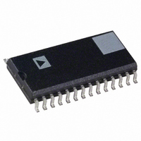
ADMCF341BR Analog Devices Inc, ADMCF341BR Datasheet - Page 23

ADMCF341BR
Manufacturer Part Number
ADMCF341BR
Description
IC DSP 3CH 12BIT MOT-CTRL 28SOIC
Manufacturer
Analog Devices Inc
Series
Motor Controlr
Type
Motor Controlr
Datasheet
1.ADMCF341BR.pdf
(36 pages)
Specifications of ADMCF341BR
Rohs Status
RoHS non-compliant
Interface
Synchronous Serial Port (SSP)
Clock Rate
20MHz
Non-volatile Memory
FLASH (12 kB), ROM (12kB)
On-chip Ram
2.5kB
Voltage - I/o
5.00V
Voltage - Core
5.00V
Operating Temperature
-40°C ~ 85°C
Mounting Type
Surface Mount
Package / Case
28-SOIC (7.5mm Width)
Available stocks
Company
Part Number
Manufacturer
Quantity
Price
Part Number:
ADMCF341BRZ
Manufacturer:
ADI/亚德诺
Quantity:
20 000
Interrupt Configuration
The IFC and ICNTL registers of the DSP core control and
configure the interrupt controller of the DSP core. The IFC
register is a 16-bit register that may be used to force and/or clear
any of the eight DSP interrupts. Bits 0 to 7 of the IFC register
may be used to clear the DSP interrupts while Bits 8 to 15 can be
used to force a corresponding interrupt. Writing to Bits 11 and
12 in IFC is the only way to create the two software interrupts.
The ICNTL register is used to configure the sensitivity (edge or
level) of the IRQ0, IRQ1, and IRQ2 interrupts and to enable/
disable interrupt nesting. Setting Bit 0 of ICNTL configures the
IRQ0 as edge-sensitive, while clearing the bit configures it as
level-sensitive. Bit 1 is used to configure the IRQ1 interrupt, and
Bit 2 is used to configure the IRQ2 interrupt. It is recommended
that the IRQ2 interrupt always be configured as level-sensi-
tive, as this ensures that no peripheral interrupts are lost. Setting
Bit 4 of the ICNTL register enables interrupt nesting. The con-
figuration of both IFC and ICNTL registers is shown in Figure 30.
INTERRUPT OPERATION
Following a reset, the ROM code on the ADMC(F)341 must
copy a default interrupt vector table into program memory
RAM from address 0x0000 to address 0x002F. Since each
interrupt source has a dedicated four-word space in this vector
table, it is possible to code short interrupt service routines (ISR)
in place. Alternatively, it may be necessary to insert a JUMP
instruction to the appropriate start address of the ISR if the ISR
requires more memory. When an interrupt occurs, the program
sequencer ensures that there is no latency (beyond synchronization
delay) when processing unmasked interrupts. In the case of the
timer, SPORT0, SPORT1, and software interrupts, the interrupt
controller automatically jumps to the appropriate location in the
interrupt vector table. At this point, a JUMP instruction to the
appropriate ISR is required. Motor control peripheral interrupts
are slightly different. When a peripheral interrupt is detected,
a bit is set in the IRQFLAG register for PWMSYNC and
PWMTRIP or in the PORTA_FLAG register for a PIO inter-
rupt, and the IRQ2 line is pulled low until all pending interrupts
are acknowledged. The DSP software must determine the source
of the interrupts by reading the IRQFLAG register. If more than
one interrupt occurs simultaneously, the higher priority interrupt
service routine is executed. Reading the IRQFLAG register
clears the PWMTRIP and PWMSYNC bits and acknowledges
the interrupt, thus allowing further interrupts when the ISR
exits. A user’s PIO interrupt service routine must read the
PORTA_FLAG register to determine which PIO port is the
source of the interrupt. Reading register PORTA_FLAG clears
all bits in the registers and acknowledges the interrupt, thus
allowing further interrupts after the ISR exits. The configuration
of all these registers is shown in Figures 26 and 29.
REV. B
–23–
SYSTEM CONTROLLER
The system controller block of the ADMC(F)341 performs the
following functions:
10. Performs a reset of the motor control peripherals and
SPORT1 and SPORT0 Control
The ADMC(F)341 has two serial ports: SPORT0 and SPORT1.
SPORT1 is available with a limited number of pins and is mainly
intended as a secondary port for development tools interfacing
and/or code booting from, as well as for external serial
memory. Figure 19 shows the internal multiplexing of the
SPORT0 and SPORT1 signals. SPORT0 is intended as a
general-purpose communication port. SPORT0 can support
the following operating modes: SPORT, UART, and SPI.
SPORT1 Configuration
There are two operating modes for SPORT1: boot mode and
UART mode. These modes are selectable through Bit 4 of the
MODECTRL register. With SPORT1 in boot mode, the
SPORT1 serial clock (SCLK1) is externally available through
the SCLK1/SCLK0 pin. The signal SCLK1 is used to drive the
external serial memory input clock.
The SPORT1 flag signal (FL1) is externally available through
the FL1/DT1 pin. This signal is used to drive the external serial
memory input reset.
With SPORT1 configured in UART mode, the SPORT0 serial
clock (SCLK0) is externally available through the SCLK1/SCLK0
pin. The SPORT1 data transmit (DT1) is externally available
through the FL1/DT1 pin.
SPORT0 Configuration
SPORT0 can be configured in the following modes: SPORT
mode, UART mode, and SPI mode.
SPORT0 can be configured for UART mode. In this mode, the DR0
and RFS0 signals of the internal serial port are connected together.
SPORT0 can be configured to operate as the master SPI inter-
face. The SPI mode is set through Bit 14 of the MODECTRL
register. When SPORT0 is configured as the SPI interface, the
SPORT I/O pins assume the configuration shown in Table XI.
1.
2.
3.
4.
5.
6.
7.
8.
9.
Manages the interface and data transfer between the DSP
core and the motor control peripherals.
Handles interrupts generated by the motor control periph-
erals and generates a DSP core interrupt signal IRQ2.
Controls the ADC multiplexer select lines.
Enables PWMTRIP and PWMSYNC interrupts.
Controls the multiplexing of the SPORT1 and SPORT0
pins.
Controls the PWM single/double update mode.
Controls the ADC conversion time modes and the SHA
timers.
Controls the auxiliary PWM operation mode.
Contains a status register (SYSSTAT) that indicates the
state of the PWMTRIP pin, the watchdog timer, and the
PWM timer.
control registers following a hardware, software, or watch-
dog initiated reset.
ADMC(F)341


