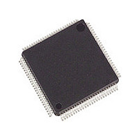
ADSP-2185MKST-300 Analog Devices Inc, ADSP-2185MKST-300 Datasheet - Page 12

ADSP-2185MKST-300
Manufacturer Part Number
ADSP-2185MKST-300
Description
IC DSP CONTROLLER 16BIT 100LQFP
Manufacturer
Analog Devices Inc
Series
ADSP-21xxr
Type
Fixed Pointr
Datasheet
1.ADSP-2185MBSTZ-266.pdf
(40 pages)
Specifications of ADSP-2185MKST-300
Rohs Status
RoHS non-compliant
Interface
Host Interface, Serial Port
Clock Rate
75MHz
Non-volatile Memory
External
On-chip Ram
80kB
Voltage - I/o
3.30V
Voltage - Core
2.50V
Operating Temperature
0°C ~ 70°C
Mounting Type
Surface Mount
Package / Case
100-LQFP
Device Core Size
16b
Architecture
Enhanced Harvard
Format
Fixed Point
Clock Freq (max)
75MHz
Mips
75
Device Input Clock Speed
75MHz
Ram Size
80KB
Program Memory Size
Not RequiredKB
Operating Supply Voltage (typ)
2.5/3.3V
Operating Supply Voltage (min)
2.37V
Operating Supply Voltage (max)
2.63/3.6V
Operating Temp Range
0C to 70C
Operating Temperature Classification
Commercial
Mounting
Surface Mount
Pin Count
100
Package Type
LQFP
Lead Free Status / Rohs Status
Not Compliant
Available stocks
Company
Part Number
Manufacturer
Quantity
Price
Company:
Part Number:
ADSP-2185MKST-300
Manufacturer:
ADI
Quantity:
300
Part Number:
ADSP-2185MKST-300
Manufacturer:
ADI/亚德诺
Quantity:
20 000
PMOVLAY
0
1
2
Active Configuration
Active Configuration involves the use of a three-statable external
driver connected to the Mode C pin. A driver’s output enable
should be connected to the DSP’s RESET signal such that it
only drives the PF2 pin when RESET is active (low). When
RESET is deasserted, the driver should three-state, thus allow-
ing full use of the PF2 pin as either an input or output. To
minimize power consumption during power-down, configure
the programmable flag as an output when connected to a three-
stated buffer. This ensures that the pin will be held at a constant
level, and will not oscillate should the three-state driver’s level
hover around the logic switching point.
IACK Configuration
Mode D = 0 and in host mode: IACK is an active, driven signal
and cannot be “wire OR’d.”
Mode D = 1 and in host mode: IACK is an open drain and
requires an external pull-down, but multiple IACK pins can be
“wire OR’d” together.
ADSP-2185M
Memory
Internal
External Overlay 1
External Overlay 2
EXTERNAL
MEMORY
ALWAYS
ACCESSIBLE
AT ADDRESS
0x0000 – 0x1FFF
ACCESSIBLE WHEN
PMOVLAY = 0
PM (MODE B = 0)
PROGRAM MEMORY
PMOVLAY = 1, 2
ACCESSIBLE WHEN
PMOVLAY = 1
8K EXTERNAL
8K INTERNAL
PMOVLAY = 0
INTERNAL
MODE B = 0
8K
OR
ACCESSIBLE WHEN
PMOVLAY = 2
0x2000 –
0x3FFF
ADDRESS
0 x 3FFF
0 x 2000
0 x 1FFF
0 x 0000
0 x 2000 –
0 x 3FFF
Table III. PMOVLAY Bits
A13
Not Applicable
0
1
0 x 2000 –
0 x 3FFF
2
2
PM (MODE B = 1)
RESERVED
MEMORY ARCHITECTURE
The ADSP-2185M provides a variety of memory and peripheral
interface options. The key functional groups are Program Memory,
Data Memory, Byte Memory, and I/O. Refer to the following
figures and tables for PM and DM memory allocations in the
ADSP-2185M.
Program Memory
Program Memory (Full Memory Mode) is a 24-bit-wide
space for storing both instruction opcodes and data. The ADSP-
2185M has 16K words of Program Memory RAM on chip, and
the capability of accessing up to two 8K external memory over-
lay spaces using the external data bus.
Program Memory (Host Mode) allows access to all internal
memory. External overlay access is limited by a single external
address line (A0). External program execution is not available in
host mode due to a restricted data bus that is 16 bits wide only.
ACCESSIBLE WHEN
PMOVLAY = 0
EXTERNAL
MEMORY
NOTES:
1
2
WHEN MODE B = 1, PMOVLAY MUST BE SET TO 0
SEE TABLE III FOR PMOVLAY BITS
PROGRAM MEMORY
1
8K INTERNAL
PMOVLAY = 0
ACCESSIBLE WHEN
PMOVLAY = 0
MODE B = 1
EXTERNAL
A12:0
Not Applicable
13 LSBs of Address Between 0x2000 and 0x3FFF
13 LSBs of Address Between 0x2000 and 0x3FFF
8K
RESERVED
0x2000 –
0x3FFF
ADDRESS
0 x 3FFF
0 x 2000
0 x 1FFF
0 x 0000
0 x 0000 –
0 x 1FFF
0 x 0000 –
0 x 1FFF
2
2


