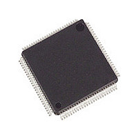
ADSP-2185MKST-300 Analog Devices Inc, ADSP-2185MKST-300 Datasheet - Page 20

ADSP-2185MKST-300
Manufacturer Part Number
ADSP-2185MKST-300
Description
IC DSP CONTROLLER 16BIT 100LQFP
Manufacturer
Analog Devices Inc
Series
ADSP-21xxr
Type
Fixed Pointr
Datasheet
1.ADSP-2185MBSTZ-266.pdf
(40 pages)
Specifications of ADSP-2185MKST-300
Rohs Status
RoHS non-compliant
Interface
Host Interface, Serial Port
Clock Rate
75MHz
Non-volatile Memory
External
On-chip Ram
80kB
Voltage - I/o
3.30V
Voltage - Core
2.50V
Operating Temperature
0°C ~ 70°C
Mounting Type
Surface Mount
Package / Case
100-LQFP
Device Core Size
16b
Architecture
Enhanced Harvard
Format
Fixed Point
Clock Freq (max)
75MHz
Mips
75
Device Input Clock Speed
75MHz
Ram Size
80KB
Program Memory Size
Not RequiredKB
Operating Supply Voltage (typ)
2.5/3.3V
Operating Supply Voltage (min)
2.37V
Operating Supply Voltage (max)
2.63/3.6V
Operating Temp Range
0C to 70C
Operating Temperature Classification
Commercial
Mounting
Surface Mount
Pin Count
100
Package Type
LQFP
Lead Free Status / Rohs Status
Not Compliant
Available stocks
Company
Part Number
Manufacturer
Quantity
Price
Company:
Part Number:
ADSP-2185MKST-300
Manufacturer:
ADI
Quantity:
300
Part Number:
ADSP-2185MKST-300
Manufacturer:
ADI/亚德诺
Quantity:
20 000
FREQUENCY DEPENDENCY FOR TIMING
SPECIFICATIONS
t
with a frequency equal to half the instruction rate. For example,
a 37.50 MHz input clock (which is equivalent to 26.6 ns) yields
a 13.3 ns processor cycle (equivalent to 75 MHz). t
within the range of 0.5 t
relevant timing parameters to obtain the specification value.
Example: t
ENVIRONMENTAL CONDITIONS
Rating
Description
Thermal Resistance
Thermal Resistance
Thermal Resistance
NOTE
1
POWER DISSIPATION
To determine total power dissipation in a specific application,
the following equation should be applied for each output:
C = load capacitance, f = output switching frequency.
Example:
In an application where external data memory is used and no other
outputs are active, power dissipation is calculated as follows:
Assumptions:
• External data memory is accessed every cycle with 50% of the
• External data memory writes occur every other cycle with
ADSP-2185M
CK
Where the Ambient Temperature Rating (T
T
T
PD = Power Dissipation in W
AMB
CASE
(Case-to-Ambient)
(Junction-to-Ambient)
(Junction-to-Case)
address pins switching.
50% of the data pins switching.
is defined as 0.5 t
= T
= Case Temperature in °C
CASE
CKH
– (PD × θ
= 0.5 t
CKI
CA
)
CK
. The ADSP-2185M uses an input clock
CKI
– 2 ns = 0.5 (15 ns) – 2 ns = 5.5 ns
C × V
Symbol
θ
θ
θ
period should be substituted for all
CA
JA
JC
DD
2 × f
AMB
1
) is:
LQFP
48°C/W
50°C/W
2°C/W
CK
Mini-BGA
63.3°C/W
70.7°C/W
7.4°C/W
values
• Each address and data pin has a 10 pF total load at the pin.
• The application operates at V
Total Power Dissipation = P
P
(C × V
Parameters
Address
Data Output, WR
RD
CLKOUT, DMS
Total power dissipation for this example is P
Output Drive Currents
Figure 14 shows typical I-V characteristics for the output drivers
on the ADSP-2185M. The curves represent the current drive
capability of the output drivers as a function of output voltage.
INT
graph (Figure 15).
= internal power dissipation from Power vs. Frequency
DDEXT
–20
–40
–60
–80
80
60
40
20
0
0
2
× f ) is calculated for each output:
V
V
V
0.5
DDEXT
DDEXT
DDEXT
= 3.3V @ +25 C
= 2.5V @ +85 C
= 3.6V @ –40 C
# of
Pins
7
9
1
2
1.0
V
OL
SOURCE VOLTAGE – V
INT
1.5
V
+ (C × V
pF
10
10
10
10
DDEXT
DDEXT
C
2.0
V
DDEXT
V
= 3.6V @ –40 C
OH
V
V
3.3
3.3
3.3
3.3
= 3.3 V and t
2.5
DDEXT
DDEXT
= 2.5V @ +85 C
V
2
2
2
2
DDEXT
= 3.3V @ +25 C
INT
3.0
2
× f )
2
+ 38.0 mW.
3.5
MHz
16.67
16.67
16.67
33.3
CK
f
= 30 ns.
4.0
PD
mW
12.7
16.3
38.0
1.8
7.2


