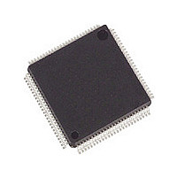
ADSP-2185MKST-300 Analog Devices Inc, ADSP-2185MKST-300 Datasheet - Page 18

ADSP-2185MKST-300
Manufacturer Part Number
ADSP-2185MKST-300
Description
IC DSP CONTROLLER 16BIT 100LQFP
Manufacturer
Analog Devices Inc
Series
ADSP-21xxr
Type
Fixed Pointr
Datasheet
1.ADSP-2185MBSTZ-266.pdf
(40 pages)
Specifications of ADSP-2185MKST-300
Rohs Status
RoHS non-compliant
Interface
Host Interface, Serial Port
Clock Rate
75MHz
Non-volatile Memory
External
On-chip Ram
80kB
Voltage - I/o
3.30V
Voltage - Core
2.50V
Operating Temperature
0°C ~ 70°C
Mounting Type
Surface Mount
Package / Case
100-LQFP
Device Core Size
16b
Architecture
Enhanced Harvard
Format
Fixed Point
Clock Freq (max)
75MHz
Mips
75
Device Input Clock Speed
75MHz
Ram Size
80KB
Program Memory Size
Not RequiredKB
Operating Supply Voltage (typ)
2.5/3.3V
Operating Supply Voltage (min)
2.37V
Operating Supply Voltage (max)
2.63/3.6V
Operating Temp Range
0C to 70C
Operating Temperature Classification
Commercial
Mounting
Surface Mount
Pin Count
100
Package Type
LQFP
Lead Free Status / Rohs Status
Not Compliant
Available stocks
Company
Part Number
Manufacturer
Quantity
Price
Company:
Part Number:
ADSP-2185MKST-300
Manufacturer:
ADI
Quantity:
300
Part Number:
ADSP-2185MKST-300
Manufacturer:
ADI/亚德诺
Quantity:
20 000
ADSP-2185M–SPECIFICATIONS
RECOMMENDED OPERATING CONDITIONS
Parameter
V
V
V
T
NOTES
1
Specifications subject to change without notice.
ELECTRICAL CHARACTERISTICS
Parameter
V
V
V
V
V
I
I
I
I
I
I
I
I
I
C
C
NOTES
10
11
12
13
Specifications subject to change without notice.
1
2
3
4
5
6
7
8
9
The ADSP-2185M is 3.3 V tolerant (always accepts up to 3.6 V max V
≈ V
BR, DR0, DR1, PWD).
IH
IL
OZH
OZL
DD
DD
DD
DD
DD
Bidirectional pins: D0–D23, RFS0, RFS1, SCLK0, SCLK1, TFS0, TFS1, A1–A13, PF0–PF7.
Input only pins: RESET, BR, DR0, DR1, PWD.
Input only pins: CLKIN, RESET, BR, DR0, DR1, PWD.
Output pins: BG, PMS, DMS, BMS, IOMS, CMS, RD, WR, PWDACK, A0, DT0, DT1, CLKOUT, FL2–0, BGH.
Although specified for TTL outputs, all ADSP-2185M outputs are CMOS-compatible and will drive to V
Guaranteed but not tested.
Three-statable pins: A0–A13, D0–D23, PMS, DMS, BMS, IOMS, CMS, RD, WR, DT0, DT1, SCLK0, SCLK1, TFS0, TFS1, RFS0, RFS1, PF0–PF7.
0 V on BR.
Idle refers to ADSP-2185M state of operation during execution of IDLE instruction. Deasserted pins are driven to either V
I
and Type 6, and 20% are idle instructions.
V
See Chapter 9 of the ADSP-2100 Family User’s Manual for details.
Output pin capacitance is the capacitive load for any three-stated output pin.
DDINT
DDEXT
INPUT
IH
IH
IL
OH
OL
AMB
I
O
DD
IN
DDEXT
measurement taken with all instructions executing from internal memory. 50% of the instructions are multifunction (Types 1, 4, 5, 12, 13, 14), 30% are Type 2
= 0 V and 3 V. For typical figures for supply currents, refer to Power Dissipation section.
1
Hi-Level Input Voltage
Hi-Level CLKIN Voltage
Lo-Level Input Voltage
Hi-Level Output Voltage
Lo-Level Output Voltage
Hi-Level Input Current
Lo-Level Input Current
Three-State Leakage Current
Three-State Leakage Current
Supply Current (Idle)
Supply Current (Idle)
Supply Current (Dynamic)
Supply Current (Dynamic)
Supply Current (Power-Down)
Input Pin Capacitance
Output Pin Capacitance
(max). This applies to bidirectional pins (D0–D23, RFS0, RFS1, SCLK0, SCLK1, TFS 0, TFS1, A1–A13, PF0–PF7) and input only pins (CLKIN, RESET,
9
9
3, 6
1, 2
1, 3
3
3
6, 7, 12, 13
1, 4, 5
1, 4, 5
10
10
7
7
Min
2.37
2.37
V
0
12
IL
= –0.3
Test Conditions
@ V
@ V
@ V
@ V
@ V
@ V
@ V
@ V
@ V
@ V
@ V
@ V
@ V
@ V
@ V
@ V
Power Mode
@ V
@ V
K Grade
DDINT
DDINT
DDINT
DDEXT
DDEXT
DDEXT
DDEXT
DDINT
DDINT
DDEXT
DDEXT
DDINT
DDINT
DDINT
DDINT
DDINT
IN
IN
= 2.5 V, f
= 2.5 V, f
= max, V
= max, V
= 2.5, t
= 2.5, t
= max
= max
= min
= 2.5, t
= 2.5, t
= 2.5, T
= min, I
= 3.0 V, I
= min, I
= min, I
= max, V
= max, V
IH
), but voltage compliance (on outputs, V
IN
IN
Max
2.63
3.6
V
+70
CK
CK
CK
CK
IH
AMB
= 1.0 MHz, T
= 1.0 MHz, T
OH
OH
OL
IN
IN
IN
IN
OH
= +3.6
= 15 ns
= 13.3 ns
= 15 ns
= 13.3 ns
= 2 mA
= –0.5 mA
= –100 µA
= 3.6 V
= 0 V
= 3.6 V
= 0 V
= 25°C in Lowest
= –0.5 mA
8
11
8
, T
11
, T
6
AMB
AMB
AMB
AMB
= 25°C
= 25°C
= 25°C
Min
2.25
2.25
V
–40
= 25°C
IL
DDEXT
= –0.3
OH
and GND, assuming no dc loads.
B Grade
) depends on the input V
Min
1.5
2.0
2.0
2.4
V
DDEXT
DD
– 0.3
K/B Grades
or GND.
Max
2.75
3.6
V
+85
IH
Typ
9
10
35
38
100
= +3.6
DDEXT
; because V
Max
0.7
0.4
10
10
10
10
8
8
OH
Unit
V
V
V
°C
Unit
V
V
V
V
V
V
V
µA
µA
µA
µA
mA
mA
mA
mA
µA
pF
pF
(max)


