EP3C16U484C6N Altera, EP3C16U484C6N Datasheet - Page 52
EP3C16U484C6N
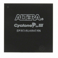
Manufacturer Part Number
EP3C16U484C6N
Description
IC CYCLONE III FPGA 16K 484UBGA
Manufacturer
Altera
Series
Cyclone® IIIr
Datasheets
1.EP3C5F256C8N.pdf
(5 pages)
2.EP3C5F256C8N.pdf
(34 pages)
3.EP3C5F256C8N.pdf
(66 pages)
4.EP3C5F256C8N.pdf
(14 pages)
5.EP3C5F256C8N.pdf
(76 pages)
Specifications of EP3C16U484C6N
Number Of Logic Elements/cells
15408
Number Of Labs/clbs
963
Total Ram Bits
516096
Number Of I /o
346
Voltage - Supply
1.15 V ~ 1.25 V
Mounting Type
Surface Mount
Operating Temperature
0°C ~ 85°C
Package / Case
484-UBGA
For Use With
544-2601 - KIT DEV CYCLONE III LS EP3CLS200P0037 - BOARD DEV/EDUCATION ALTERA DE0544-2411 - KIT DEV NIOS II CYCLONE III ED.
Lead Free Status / RoHS Status
Lead free / RoHS Compliant
Number Of Gates
-
Other names
544-2478
Available stocks
Company
Part Number
Manufacturer
Quantity
Price
Company:

Part Number:
EP3C16U484C6N
Manufacturer:
IDT
Quantity:
247
Company:
Part Number:
EP3C16U484C6N
Manufacturer:
ALTERA
Quantity:
147
Part Number:
EP3C16U484C6N
Manufacturer:
ALTERA
Quantity:
20 000


2–8
Cyclone III Device Handbook, Volume 2
Table 2–9. Cyclone III LS Devices Pin Capacitance (Part 2 of 2)
C
C
C
C
Note to
(1) When you use the VREF pin as a regular input or output, you can expect a reduced performance of toggle rate and
Symbol
V REFLR
V REFTB
C LKTB
C LKLR
t
C O
(1)
(1)
due to higher pin capacitance.
Table
Input capacitance on left/right dual-purpose VREF pin
when used as V
Input capacitance on top/bottom dual-purpose VREF
pin when used as V
Input capacitance on top/bottom dedicated clock input
pins
Input capacitance on left/right dedicated clock input
pins
2–9:
REF
or user I/O pin
REF
Parameter
or user I/O pin
Chapter 2: Cyclone III LS Device Data Sheet
© December 2009 Altera Corporation
Typical –
QFP
21
23
7
6
Electrical Characteristics
Typical –
FBGA
21
23
6
5
Unit
pF
pF
pF
pF
Related parts for EP3C16U484C6N
Image
Part Number
Description
Manufacturer
Datasheet
Request
R

Part Number:
Description:
CYCLONE II STARTER KIT EP2C20N
Manufacturer:
Altera
Datasheet:


Part Number:
Description:
CPLD, EP610 Family, ECMOS Process, 300 Gates, 16 Macro Cells, 16 Reg., 16 User I/Os, 5V Supply, 35 Speed Grade, 24DIP
Manufacturer:
Altera Corporation
Datasheet:
Part Number:
Description:
CPLD, EP610 Family, ECMOS Process, 300 Gates, 16 Macro Cells, 16 Reg., 16 User I/Os, 5V Supply, 15 Speed Grade, 24DIP
Manufacturer:
Altera Corporation
Datasheet:
Part Number:
Description:
Manufacturer:
Altera Corporation
Datasheet:
Part Number:
Description:
CPLD, EP610 Family, ECMOS Process, 300 Gates, 16 Macro Cells, 16 Reg., 16 User I/Os, 5V Supply, 30 Speed Grade, 24DIP
Manufacturer:
Altera Corporation
Datasheet:
Part Number:
Description:
High-performance, low-power erasable programmable logic devices with 8 macrocells, 10ns
Manufacturer:
Altera Corporation
Datasheet:
Part Number:
Description:
High-performance, low-power erasable programmable logic devices with 8 macrocells, 7ns
Manufacturer:
Altera Corporation
Datasheet:
Part Number:
Description:
Classic EPLD
Manufacturer:
Altera Corporation
Datasheet:
Part Number:
Description:
High-performance, low-power erasable programmable logic devices with 8 macrocells, 10ns
Manufacturer:
Altera Corporation
Datasheet:
Part Number:
Description:
Manufacturer:
Altera Corporation
Datasheet:
Part Number:
Description:
Manufacturer:
Altera Corporation
Datasheet:
Part Number:
Description:
Manufacturer:
Altera Corporation
Datasheet:
Part Number:
Description:
CPLD, EP610 Family, ECMOS Process, 300 Gates, 16 Macro Cells, 16 Reg., 16 User I/Os, 5V Supply, 25 Speed Grade, 24DIP
Manufacturer:
Altera Corporation
Datasheet: