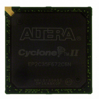
EP2C35F672C6N Altera, EP2C35F672C6N Datasheet - Page 146

EP2C35F672C6N
Manufacturer Part Number
EP2C35F672C6N
Description
IC CYCLONE II FPGA 33K 672-FBGA
Manufacturer
Altera
Series
Cyclone® IIr
Datasheet
1.EP2C5T144C8N.pdf
(168 pages)
Specifications of EP2C35F672C6N
Number Of Logic Elements/cells
33216
Number Of Labs/clbs
2076
Total Ram Bits
483840
Number Of I /o
475
Voltage - Supply
1.15 V ~ 1.25 V
Mounting Type
Surface Mount
Operating Temperature
0°C ~ 85°C
Package / Case
672-FBGA
Family Name
Cyclone® II
Number Of Logic Blocks/elements
33216
# I/os (max)
475
Frequency (max)
500MHz
Process Technology
90nm
Operating Supply Voltage (typ)
1.2V
Logic Cells
33216
Ram Bits
483840
Operating Supply Voltage (min)
1.15V
Operating Supply Voltage (max)
1.25V
Operating Temp Range
0C to 85C
Operating Temperature Classification
Commercial
Mounting
Surface Mount
Pin Count
672
Package Type
FBGA
For Use With
P0301 - DE2 CALL FOR ACADEMIC PRICING544-1733 - PCI KIT W/CYCLONE II EP2C35N649-1001 - KIT DEV CYCLONE II PCI EXPRESS
Lead Free Status / RoHS Status
Lead free / RoHS Compliant
Number Of Gates
-
Lead Free Status / Rohs Status
Compliant
Other names
544-1694
Available stocks
Company
Part Number
Manufacturer
Quantity
Price
Company:
Part Number:
EP2C35F672C6N
Manufacturer:
ALTERA
Quantity:
170
Timing Specifications
Figure 5–3. High-Speed I/O Timing Diagram
5–56
Cyclone II Device Handbook, Volume 1
Sampling window
Receiver input skew
margin
Input jitter (peak to peak)
Output jitter (peak to peak)
Signal rise time
Signal fall time
Lock time
Table 5–47. High-Speed I/O Timing Definitions (Part 2 of 2)
Parameter
Internal Clock
Input Clock
Input Data
Receiver
External
SW
RSKM
t
t
t
R I S E
FA L L
L O C K
Symbol
Figure 5–4
TCCS
—
—
The period of time during which the data must be valid in order for you
to capture it correctly. Sampling window is the sum of the setup time,
hold time, and jitter. The window of t
in the sampling window.
SW = TUI – TCCS – (2 × RSKM)
RSKM is defined by the total margin left after accounting for the
sampling window and TCCS.
RSKM = (TUI – SW – TCCS) / 2
Peak-to-peak input jitter on high-speed PLLs.
Peak-to-peak output jitter on high-speed PLLs.
Low-to-high transmission time.
High-to-low transmission time.
Lock time for high-speed transmitter and receiver PLLs.
RSKM
shows the high-speed I/O timing budget.
Sampling Window (SW)
Time Unit Interval (TUI)
Description
SU
RSKM
+ t
H
is expected to be centered
TCCS
Altera Corporation
February 2008


