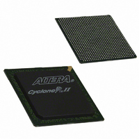
EP2C70F896I8N Altera, EP2C70F896I8N Datasheet - Page 58

EP2C70F896I8N
Manufacturer Part Number
EP2C70F896I8N
Description
IC CYCLONE II FPGA 70K 896-FBGA
Manufacturer
Altera
Series
Cyclone® IIr
Datasheet
1.EP2C5T144C8N.pdf
(168 pages)
Specifications of EP2C70F896I8N
Number Of Logic Elements/cells
68416
Number Of Labs/clbs
4276
Total Ram Bits
1152000
Number Of I /o
622
Voltage - Supply
1.15 V ~ 1.25 V
Mounting Type
Surface Mount
Operating Temperature
-40°C ~ 100°C
Package / Case
896-FBGA
Family Name
Cyclone® II
Number Of Logic Blocks/elements
68416
# I/os (max)
622
Frequency (max)
402.58MHz
Process Technology
90nm
Operating Supply Voltage (typ)
1.2V
Logic Cells
68416
Ram Bits
1152000
Operating Supply Voltage (min)
1.15V
Operating Supply Voltage (max)
1.25V
Operating Temp Range
-40C to 100C
Operating Temperature Classification
Industrial
Mounting
Surface Mount
Pin Count
896
Package Type
FBGA
For Use With
P0304 - DE2-70 CALL FOR ACADEMIC PRICING544-1703 - VIDEO KIT W/CYCLONE II EP2C70N544-1699 - DSP KIT W/CYCLONE II EPS2C70N
Lead Free Status / RoHS Status
Lead free / RoHS Compliant
Number Of Gates
-
Lead Free Status / Rohs Status
Compliant
Other names
544-2147
Available stocks
Company
Part Number
Manufacturer
Quantity
Price
Company:
Part Number:
EP2C70F896I8N
Manufacturer:
ALTERA21
Quantity:
196
Part Number:
EP2C70F896I8N
Manufacturer:
ALTERA/阿尔特拉
Quantity:
20 000
I/O Structure & Features
Figure 2–26. Cyclone II Device DQ & DQS Groups in ×8/×9 Mode
Notes to
(1)
(2)
2–46
Cyclone II Device Handbook, Volume 1
EP2C5
EP2C8
EP2C15
EP2C20
Table 2–15. Cyclone II DQS & DQ Bus Mode Support (Part 1 of 2)
Device
Each DQ group consists of a DQS pin, DM pin, and up to nine DQ pins.
This is an idealized pin layout. For actual pin layout, refer to the pin table.
Figure
2–26:
144-pin TQFP
208-pin PQFP
144-pin TQFP
208-pin PQFP
256-pin FineLine BGA
256-pin FineLine BGA
484-pin FineLine BGA
256-pin FineLine BGA
484-pin FineLine BGA
DQ Pins
Package
Cyclone II devices support the data strobe or read clock signal (DQS)
used in DDR and DDR2 SDRAM. Cyclone II devices can use either
bidirectional data strobes or unidirectional read clocks. The dedicated
external memory interface in Cyclone II devices also includes
programmable delay circuitry that can shift the incoming DQS signals to
center align the DQS signals within the data window.
The DQS signal is usually associated with a group of data (DQ) pins. The
phase-shifted DQS signals drive the global clock network, which is used
to clock the DQ signals on internal LE registers.
Table 2–15
(2)
(2)
®
shows the number of DQ pin groups per device.
Number of ×8
Groups
16
16
7
7
8
3
3
8
8
(3)
(3)
(3)
(4)
(4)
DQS Pin
Groups (5),
(2)
Number of ×9
3
4
3
4
4
4
8
4
8
Notes
(6)
Note (1)
(1),
DQ Pins
Number of ×16
(2)
Groups
0
3
0
3
4
4
8
4
8
Altera Corporation
Number of ×18
Groups (5),
February 2007
DM Pin
0
3
0
3
4
4
8
4
8
(6)


