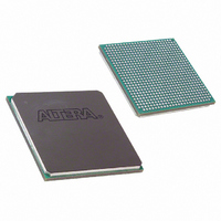
EP2S60F672I4N Altera, EP2S60F672I4N Datasheet - Page 86

EP2S60F672I4N
Manufacturer Part Number
EP2S60F672I4N
Description
IC STRATIX II FPGA 60K 672-FBGA
Manufacturer
Altera
Series
Stratix® IIr
Datasheet
1.EP2S15F484I4N.pdf
(238 pages)
Specifications of EP2S60F672I4N
Number Of Logic Elements/cells
60440
Number Of Labs/clbs
3022
Total Ram Bits
2544192
Number Of I /o
492
Voltage - Supply
1.15 V ~ 1.25 V
Mounting Type
Surface Mount
Operating Temperature
-40°C ~ 100°C
Package / Case
672-FBGA
For Use With
544-1700 - DSP KIT W/STRATIX II EP2S60N544-1697 - NIOS II KIT W/STRATIX II EP2S60N
Lead Free Status / RoHS Status
Lead free / RoHS Compliant
Number Of Gates
-
Other names
544-1916
EP2S60F672I4N
EP2S60F672I4N
Available stocks
Company
Part Number
Manufacturer
Quantity
Price
Company:
Part Number:
EP2S60F672I4N
Manufacturer:
ALTERA
Quantity:
201
Company:
Part Number:
EP2S60F672I4N
Manufacturer:
ALTERA
Quantity:
400
Part Number:
EP2S60F672I4N
Manufacturer:
ALTERA/阿尔特拉
Quantity:
20 000
I/O Structure
Figure 2–52. Stratix II IOE in DDR Input I/O Configuration
Notes to
(1)
(2)
(3)
(4)
2–78
Stratix II Device Handbook, Volume 1
Column, Row,
Interconnect
or Local
All input signals to the IOE can be inverted at the IOE.
This signal connection is only allowed on dedicated DQ function pins.
This signal is for dedicated DQS function pins only.
The optional PCI clamp is only available on column I/O pins.
Figure
ioe_clk[7..0]
DQS Local
2–52:
Bus (2)
sclr/spreset
clkin
ce_in
aclr/apreset
Chip-Wide Reset
When using the IOE for DDR inputs, the two input registers clock double
rate input data on alternating edges. An input latch is also used in the IOE
for DDR input acquisition. The latch holds the data that is present during
the clock high times. This allows both bits of data to be synchronous with
the same clock edge (either rising or falling).
configured for DDR input.
diagram.
Input Register
Input Register
D
CLRN/PRN
ENA
CLRN/PRN
D
ENA
Input RegisterDelay
I
nput Pin to
Q
Q
Figure 2–53
Notes
(1), (2),
D
ENA
CLRN/PRN
To DQS Logic
Latch
Block (3)
shows the DDR input timing
Q
(3)
Figure 2–52
VCCIO
VCCIO
PCI Clamp (4)
Altera Corporation
shows an IOE
Bus-Hold
Termination
Circuit
On-Chip
Programmable
Pull-Up
Resistor
May 2007


