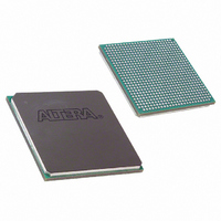
EP2S30F672C5N Altera, EP2S30F672C5N Datasheet - Page 104

EP2S30F672C5N
Manufacturer Part Number
EP2S30F672C5N
Description
IC STRATIX II FPGA 30K 672-FBGA
Manufacturer
Altera
Series
Stratix® IIr
Datasheet
1.EP2S15F484I4N.pdf
(238 pages)
Specifications of EP2S30F672C5N
Number Of Logic Elements/cells
33880
Number Of Labs/clbs
1694
Total Ram Bits
1369728
Number Of I /o
500
Voltage - Supply
1.15 V ~ 1.25 V
Mounting Type
Surface Mount
Operating Temperature
0°C ~ 85°C
Package / Case
672-FBGA
Family Name
Stratix II
Number Of Logic Blocks/elements
33880
# I/os (max)
500
Frequency (max)
609.76MHz
Process Technology
90nm (CMOS)
Operating Supply Voltage (typ)
1.2V
Logic Cells
33880
Ram Bits
1369728
Operating Supply Voltage (min)
1.15V
Operating Supply Voltage (max)
1.25V
Operating Temp Range
0C to 85C
Operating Temperature Classification
Commercial
Mounting
Surface Mount
Pin Count
672
Package Type
FC-FBGA
Family Type
Stratix II
No. Of I/o's
500
I/o Supply Voltage
3.3V
Operating Frequency Max
550MHz
Operating Temperature Range
0°C To +85°C
Logic Case Style
BGA
No. Of Pins
672
Rohs Compliant
Yes
Lead Free Status / RoHS Status
Lead free / RoHS Compliant
Number Of Gates
-
Lead Free Status / Rohs Status
Compliant
Other names
544-1898
EP2S30F672C5N
EP2S30F672C5N
Available stocks
Company
Part Number
Manufacturer
Quantity
Price
Company:
Part Number:
EP2S30F672C5N
Manufacturer:
ALTERA
Quantity:
238
Part Number:
EP2S30F672C5N
Manufacturer:
ALTERA/阿尔特拉
Quantity:
20 000
High-Speed Differential I/O with DPA Support
High-Speed
Differential I/O
with DPA
Support
2–96
Stratix II Device Handbook, Volume 1
Notes to
(1)
(2)
(3)
(4)
(5)
(6)
Non-Stratix II VCC = 3.3 V
Table 2–20. Supported TDO/TDI Voltage Combinations (Part 2 of 2)
Device
The TDO output buffer meets V
The TDO output buffer meets V
An external 250-Ω pull-up resistor is not required, but recommended if signal levels on the board are not optimal.
Input buffer must be 3.3-V tolerant.
Input buffer must be 2.5-V tolerant.
Input buffer must be 1.8-V tolerant.
Table
2–20:
VCC = 2.5 V
VCC = 1.8 V
VCC = 1.5 V
Buffer Power
TDI Input
Stratix II devices contain dedicated circuitry for supporting differential
standards at speeds up to 1 Gbps. The LVDS and HyperTransport
differential I/O standards are supported in the Stratix II device. In
addition, the LVPECL I/O standard is supported on input and output
clock pins on the top and bottom I/O banks.
The high-speed differential I/O circuitry supports the following high
speed I/O interconnect standards and applications:
■
■
■
■
There are four dedicated high-speed PLLs in the EP2S15 to EP2S30
devices and eight dedicated high-speed PLLs in the EP2S60 to EP2S180
devices to multiply reference clocks and drive high-speed differential
SERDES channels.
Tables 2–21
can clock in each of the Stratix II devices. In
first row for each transmitter or receiver provides the number of channels
driven directly by the PLL. The second row below it shows the maximum
channels a PLL can drive if cross bank channels are used from the
adjacent center PLL. For example, in the 484-pin FineLine BGA EP2S15
V
C C I O
v
v
v
OH
OH
SPI-4 Phase 2 (POS-PHY Level 4)
SFI-4
Parallel RapidIO
HyperTransport technology
v
(1),
(1),
(1),
(MIN) = 2.4 V.
(MIN) = 2.0 V.
= 3.3 V V
(1)
(4)
(4)
(4)
through
Stratix II TDO V
C C I O
v
v
v
v
2–26
(2),
(2),
= 2.5 V V
(2)
(2)
(5)
(5)
show the number of channels that each fast PLL
C C I O
C C I O
Voltage Level in I/O Bank 4
v
v
v
v
= 1.8 V V
(3)
(3)
(6)
Tables 2–21
Level shifter
Level shifter
Level shifter
C C I O
required
required
required
v
= 1.5 V V
Altera Corporation
through
Level shifter
Level shifter
Level shifter
C C I O
required
required
required
May 2007
2–26
v
= 1.2 V
the


