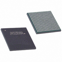
EP1C4F324I7 Altera, EP1C4F324I7 Datasheet - Page 97

EP1C4F324I7
Manufacturer Part Number
EP1C4F324I7
Description
IC CYCLONE FPGA 4K LE 324-FBGA
Manufacturer
Altera
Series
Cyclone®r
Datasheet
1.EP1C3T144C8.pdf
(106 pages)
Specifications of EP1C4F324I7
Number Of Logic Elements/cells
4000
Number Of Labs/clbs
400
Total Ram Bits
78336
Number Of I /o
249
Voltage - Supply
1.425 V ~ 1.575 V
Mounting Type
Surface Mount
Operating Temperature
-40°C ~ 100°C
Package / Case
324-FBGA
Family Name
Cyclone®
Number Of Logic Blocks/elements
4000
# I/os (max)
249
Frequency (max)
320.1MHz
Process Technology
0.13um (CMOS)
Operating Supply Voltage (typ)
1.5V
Logic Cells
4000
Ram Bits
78336
Operating Supply Voltage (min)
1.425V
Operating Supply Voltage (max)
1.575V
Operating Temp Range
-40C to 100C
Operating Temperature Classification
Industrial
Mounting
Surface Mount
Pin Count
324
Package Type
FBGA
Lead Free Status / RoHS Status
Contains lead / RoHS non-compliant
Number Of Gates
-
Lead Free Status / Rohs Status
Not Compliant
Other names
544-1045
Available stocks
Company
Part Number
Manufacturer
Quantity
Price
Company:
Part Number:
EP1C4F324I7
Manufacturer:
ALTERA41
Quantity:
742
Part Number:
EP1C4F324I7
Manufacturer:
ALTERA/阿尔特拉
Quantity:
20 000
Company:
Part Number:
EP1C4F324I7N
Manufacturer:
ALTERA
Quantity:
996
Part Number:
EP1C4F324I7N
Manufacturer:
ALTERA
Quantity:
20 000
Altera Corporation
May 2008
Note to
(1)
Decrease input delay to
internal cells
Decrease input delay to input
register
Increase delay to output pin
Table 4–47. Cyclone IOE Programmable Delays on Row Pins
EPC1C3 devices do not support the PCI I/O standard.
Table
Parameter
4–47:
Maximum Input and Output Clock Rates
Tables 4–48
row pins in Cyclone devices.
Off
Off
Small
Medium
Large
On
Off
On
On
LVTTL
2.5 V
1.8 V
1.5 V
LVCMOS
SSTL-3 class I
SSTL-3 class II
SSTL-2 class I
SSTL-2 class II
LVDS
Table 4–48. Cyclone Maximum Input Clock Rate for Column Pins
Setting
I/O Standard
and
-6 Speed Grade
Min
—
—
—
—
—
—
—
—
—
4–49
show the maximum input clock rate for column and
2,212
2,639
3,057
3,057
Max
154
154
556
0
0
-6 Speed
Grade
464
392
387
387
405
405
414
464
473
567
-7 Speed Grade
Min
—
—
—
—
—
—
—
—
—
2,543
3,034
3,515
3,515
-7 Speed
Max
177
177
639
Grade
0
0
428
302
311
320
374
356
365
428
432
549
-8 Speed Grade
Min
—
—
—
—
—
—
—
—
—
-8 Speed
Grade
387
207
252
243
333
293
302
396
396
531
3,430
2,875
3,974
3,974
Max
200
200
722
Timing Model
0
0
Preliminary
MHz
MHz
MHz
MHz
MHz
MHz
MHz
MHz
MHz
MHz
Unit
Unit
4–27
ps
ps
ps
ps
ps
ps
ps
ps
ps


