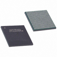
EP1C12F324I7N Altera, EP1C12F324I7N Datasheet - Page 51

EP1C12F324I7N
Manufacturer Part Number
EP1C12F324I7N
Description
IC CYCLONE FPGA 12K LE 324-FBGA
Manufacturer
Altera
Series
Cyclone®r
Datasheet
1.EP1C3T144C8.pdf
(106 pages)
Specifications of EP1C12F324I7N
Number Of Logic Elements/cells
12060
Number Of Labs/clbs
1206
Total Ram Bits
239616
Number Of I /o
249
Voltage - Supply
1.425 V ~ 1.575 V
Mounting Type
Surface Mount
Operating Temperature
-40°C ~ 100°C
Package / Case
324-FBGA
Lead Free Status / RoHS Status
Lead free / RoHS Compliant
Number Of Gates
-
Available stocks
Company
Part Number
Manufacturer
Quantity
Price
Company:
Part Number:
EP1C12F324I7N
Manufacturer:
ALTERA
Quantity:
339
Company:
Part Number:
EP1C12F324I7N
Manufacturer:
ALTERA32
Quantity:
96
Part Number:
EP1C12F324I7N
Manufacturer:
ALTERA/阿尔特拉
Quantity:
20 000
Figure 2–32. Cyclone IOE in Bidirectional I/O Configuration
Altera Corporation
May 2008
Column or Row
Interconect
ioe_clk[5..0]
comb_datain
data_in
Chip-Wide Reset
OE
clkout
aclr/prn
ce_in
ce_out
clkin
sclr/preset
The Cyclone device IOE includes programmable delays to ensure zero
hold times, minimize setup times, or increase clock to output times.
A path in which a pin directly drives a register may require a
programmable delay to ensure zero hold time, whereas a path in which a
pin drives a register through combinatorial logic may not require the
delay. Programmable delays decrease input-pin-to-logic-array and IOE
input register delays. The Quartus II Compiler can program these delays
Output Register
Input Register
OE Register
D
D
D
CLRN
CLRN
CLRN
PRN
ENA
PRN
ENA
PRN
ENA
Q
Q
Q
Pin Delay
Drive Strength Control
Output
Open-Drain Output
Slew Control
Input Register Delay
Logic Array Delay
Logic Array Delay
or Input Pin to
Input Pin to
Input Pin to
V
CCIO
V
CCIO
Optional
PCI Clamp
I/O Structure
Preliminary
Bus Hold
Programmable
Pull-Up
Resistor
2–45


