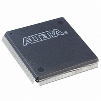
EP20K100EQC240-2 Altera, EP20K100EQC240-2 Datasheet - Page 39

EP20K100EQC240-2
Manufacturer Part Number
EP20K100EQC240-2
Description
IC APEX 20KE FPGA 100K 240-PQFP
Manufacturer
Altera
Series
APEX-20K®r
Datasheet
1.EP20K30ETC144-3.pdf
(117 pages)
Specifications of EP20K100EQC240-2
Number Of Logic Elements/cells
4160
Number Of Labs/clbs
416
Total Ram Bits
53248
Number Of I /o
183
Number Of Gates
263000
Voltage - Supply
1.71 V ~ 1.89 V
Mounting Type
Surface Mount
Operating Temperature
0°C ~ 85°C
Package / Case
240-MQFP, 240-PQFP
Lead Free Status / RoHS Status
Contains lead / RoHS non-compliant
Other names
544-1864
EP20K100EQC240-2
EP20K100EQC240-2
Available stocks
Company
Part Number
Manufacturer
Quantity
Price
Company:
Part Number:
EP20K100EQC240-2
Manufacturer:
ALTERA
Quantity:
24
Company:
Part Number:
EP20K100EQC240-2
Manufacturer:
ALTERA
Quantity:
1 831
Company:
Part Number:
EP20K100EQC240-2X
Manufacturer:
ALTERA
Quantity:
1
Altera Corporation
Figure 25. APEX 20K Bidirectional I/O Registers
Note to
(1)
or Local Interconnect
The output enable and input registers are LE registers in the LAB adjacent to the bidirectional pin.
Row, Column,
Figure
25:
4 Dedicated
Inputs
Clock Inputs
2 Dedicated
2
Peripheral Control
Bus
12
OE[7..0]
VCC
CLK[1..0]
CLK[3..2]
ENA[5..0]
CLRn[1..0]
VCC
Input Pin to Input
Core to Output
Register Delay
VCC
VCC
Register Delay
VCC
VCC
VCC
APEX 20K Programmable Logic Device Family Data Sheet
Chip-Wide
Chip-Wide
Chip-Wide Reset
Input Pin to
Reset
Reset
Core Delay
Note (1)
Output Enable
Output Register
Chip-Wide
Input Register
OE Register
D
ENA
D
ENA
D
ENA
CLRN
CLRN
CLRN
Q
Q
Q
Open-Drain
Slew-Rate
Output
Control
Output Register
t
CO
Delay
VCCIO
Optional
PCI Clamp
39


