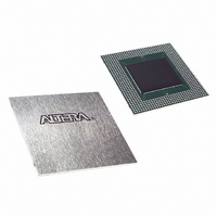
EP20K400EBC652-3N Altera, EP20K400EBC652-3N Datasheet - Page 76

EP20K400EBC652-3N
Manufacturer Part Number
EP20K400EBC652-3N
Description
IC APEX 20KE FPGA 400K 652-BGA
Manufacturer
Altera
Series
APEX-20K®r
Datasheet
1.EP20K30ETC144-3.pdf
(117 pages)
Specifications of EP20K400EBC652-3N
Number Of Logic Elements/cells
16640
Number Of Labs/clbs
1664
Total Ram Bits
212992
Number Of I /o
488
Number Of Gates
1052000
Voltage - Supply
1.71 V ~ 1.89 V
Mounting Type
Surface Mount
Operating Temperature
0°C ~ 85°C
Package / Case
652-BGA
Family Name
APEX 20K
Number Of Usable Gates
400000
Number Of Logic Blocks/elements
16640
# I/os (max)
488
Frequency (max)
213MHz
Process Technology
SRAM
Operating Supply Voltage (typ)
1.8V
Logic Cells
16640
Ram Bits
212992
Device System Gates
1052000
Operating Supply Voltage (min)
1.71V
Operating Supply Voltage (max)
1.89V
Operating Temp Range
0C to 85C
Operating Temperature Classification
Commercial
Mounting
Surface Mount
Pin Count
652
Package Type
BGA
Lead Free Status / RoHS Status
Lead free / RoHS Compliant
Available stocks
Company
Part Number
Manufacturer
Quantity
Price
APEX 20K Programmable Logic Device Family Data Sheet
Note to
(1)
76
t
t
t
t
t
t
t
t
t
t
INSUBIDIR
INHBIDIR
OUTCOBIDIR
XZBIDIR
ZXBIDIR
INSUBIDIRPLL
INHBIDIRPLL
OUTCOBIDIRPLL
XZBIDIRPLL
ZXBIDIRPLL
Table 39. APEX 20KE External Bidirectional Timing Parameters
These timing parameters are sample-tested only.
Symbol
Tables 38
and 39:
Setup time for bidirectional pins with global clock at LAB adjacent Input
Register
Hold time for bidirectional pins with global clock at LAB adjacent Input
Register
Clock-to-output delay for bidirectional pins with global clock at IOE output
register
Synchronous Output Enable Register to output buffer disable delay
Synchronous Output Enable Register output buffer enable delay
Setup time for bidirectional pins with PLL clock at LAB adjacent Input
Register
Hold time for bidirectional pins with PLL clock at LAB adjacent Input
Register
Clock-to-output delay for bidirectional pins with PLL clock at IOE output
register
Synchronous Output Enable Register to output buffer disable delay with
PLL
Synchronous Output Enable Register output buffer enable delay with PLL
Parameter
Note (1)
Altera Corporation
C1 = 10 pF
C1 = 10 pF
C1 = 10 pF
C1 = 10 pF
C1 = 10 pF
C1 = 10 pF
Conditions


