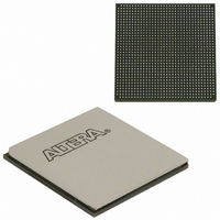
EP1AGX90EF1152C6 Altera, EP1AGX90EF1152C6 Datasheet - Page 87

EP1AGX90EF1152C6
Manufacturer Part Number
EP1AGX90EF1152C6
Description
IC ARRIA GX FPGA 90K 1152FBGA
Manufacturer
Altera
Series
Arria GXr
Datasheet
1.EP1AGX20CF484C6N.pdf
(234 pages)
Specifications of EP1AGX90EF1152C6
Number Of Logic Elements/cells
90220
Number Of Labs/clbs
4511
Total Ram Bits
4477824
Number Of I /o
538
Voltage - Supply
1.15 V ~ 1.25 V
Mounting Type
Surface Mount
Operating Temperature
0°C ~ 85°C
Package / Case
1152-FBGA
Lead Free Status / RoHS Status
Contains lead / RoHS non-compliant
Number Of Gates
-
Available stocks
Company
Part Number
Manufacturer
Quantity
Price
Company:
Part Number:
EP1AGX90EF1152C6
Manufacturer:
ALTERA
Quantity:
3 000
Company:
Part Number:
EP1AGX90EF1152C6N
Manufacturer:
ALTERA
Quantity:
3 000
Chapter 2: Arria GX Architecture
I/O Structure
Figure 2–66. Arria GX Device Fast PLL
Notes to
(1) The global or regional clock input can be driven by an output from another PLL, a pin-driven dedicated global or regional clock, or through a clock
(2) In high-speed differential I/O support mode, this high-speed PLL clock feeds the serializer/deserializer (SERDES) circuitry. Arria GX devices only
(3) This signal is a differential I/O SERDES control signal.
(4) Arria GX fast PLLs only support manual clock switchover.
I/O Structure
© December 2009 Altera Corporation
control block provided the clock control block is fed by an output from another PLL or a pin-driven dedicated global or regional clock. An internally
generated global signal cannot drive the PLL.
support one rate of data transfer per fast PLL in high-speed differential I/O support mode.
Figure
Clock
Input
f
2–66:
Global or
regional clock (1)
Global or
regional clock (1)
4
For more information about enhanced and fast PLLs, refer to the
Devices
refer to
Arria GX IOEs provide many features, including:
■
■
■
■
■
■
■
■
■
■
■
■
■
■
■
Dedicated differential and single-ended I/O buffers
3.3-V, 64-bit, 66-MHz PCI compliance
3.3-V, 64-bit, 133-MHz PCI-X 1.0 compliance
JTAG boundary-scan test (BST) support
On-chip driver series termination
OCT for differential standards
Programmable pull-up during configuration
Output drive strength control
Tri-state buffers
Bus-hold circuitry
Programmable pull-up resistors
Programmable input and output delays
Open-drain outputs
DQ and DQS I/O pins
DDR registers
Shaded Portions of the
PLL are Reconfigurable
chapter. For more information about high-speed differential I/O support,
“High-Speed Differential I/O with DPA Support” on page
Circuitry (4)
Switchover
Clock
÷n
Frequency
Detector
Phase
PFD
Charge
Pump
Loop
Filter
÷m
VCO
VCO Phase Selection
Selectable at each PLL
Output Port
÷k
8
Post-Scale
Counters
÷c0
÷c1
÷c2
÷c3
Arria GX Device Handbook, Volume 1
4
PLLs in Arria GX
4
8
8
2–99.
diffioclk0
load_en0
load_en1
diffioclk1
Global clocks
Regional clocks
to DPA block
(2)
(3)
(3)
(2)
2–81


