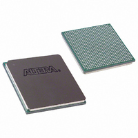
EP1S25F780C6 Altera, EP1S25F780C6 Datasheet - Page 141

EP1S25F780C6
Manufacturer Part Number
EP1S25F780C6
Description
IC STRATIX FPGA 25K LE 780-FBGA
Manufacturer
Altera
Series
Stratix®r
Datasheet
1.EP1S10F780C7.pdf
(276 pages)
Specifications of EP1S25F780C6
Number Of Logic Elements/cells
25660
Number Of Labs/clbs
2566
Total Ram Bits
1944576
Number Of I /o
597
Voltage - Supply
1.425 V ~ 1.575 V
Mounting Type
Surface Mount
Operating Temperature
0°C ~ 85°C
Package / Case
780-FBGA
Family Name
Stratix
Number Of Logic Blocks/elements
25660
# I/os (max)
597
Frequency (max)
450.05MHz
Process Technology
0.13um (CMOS)
Operating Supply Voltage (typ)
1.5V
Logic Cells
25660
Ram Bits
1944576
Operating Supply Voltage (min)
1.425V
Operating Supply Voltage (max)
1.575V
Operating Temp Range
0C to 85C
Operating Temperature Classification
Commercial
Mounting
Surface Mount
Pin Count
780
Package Type
FC-FBGA
Lead Free Status / RoHS Status
Contains lead / RoHS non-compliant
Number Of Gates
-
Lead Free Status / Rohs Status
Not Compliant
Other names
544-1121
Available stocks
Company
Part Number
Manufacturer
Quantity
Price
Company:
Part Number:
EP1S25F780C6
Manufacturer:
ALTERA
Quantity:
10
Company:
Part Number:
EP1S25F780C6
Manufacturer:
ALTERA
Quantity:
246
Part Number:
EP1S25F780C6
Manufacturer:
ALTERA/阿尔特拉
Quantity:
20 000
Part Number:
EP1S25F780C6ES
Manufacturer:
ALTERA
Quantity:
20 000
Company:
Part Number:
EP1S25F780C6N
Manufacturer:
ALTERA
Quantity:
1 045
Altera Corporation
July 2005
SSTL-3 Class II
AGP (1× and 2× )
CTT
Table 2–32. I/O Support by Bank (Part 2 of 2)
I/O Standard
Each I/O bank has its own VCCIO pins. A single device can support 1.5-,
1.8-, 2.5-, and 3.3-V interfaces; each bank can support a different standard
independently. Each bank also has dedicated VREF pins to support any
one of the voltage-referenced standards (such as SSTL-3) independently.
Each I/O bank can support multiple standards with the same V
input and output pins. Each bank can support one voltage-referenced
I/O standard. For example, when V
LVTTL, LVCMOS, 3.3-V PCI, and SSTL-3 for inputs and outputs.
Differential On-Chip Termination
Stratix devices provide differential on-chip termination (LVDS I/O
standard) to reduce reflections and maintain signal integrity. Differential
on-chip termination simplifies board design by minimizing the number
of external termination resistors required. Termination can be placed
inside the package, eliminating small stubs that can still lead to
reflections. The internal termination is designed using transistors in the
linear region of operation.
Stratix devices support internal differential termination with a nominal
resistance value of 137.5 Ω for LVDS input receiver buffers. LVPECL
signals require an external termination resistor.
device with differential termination.
Top & Bottom Banks
(3, 4, 7 & 8)
v
v
v
Left & Right Banks
(1, 2, 5 & 6)
v
v
CCIO
Stratix Device Handbook, Volume 1
is 3.3 V, a bank can support
Figure 2–71
Enhanced PLL External
Clock Output Banks
(9, 10, 11 & 12)
Stratix Architecture
v
v
v
shows the
CCIO
2–127
for


