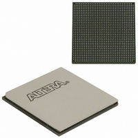
EP2SGX90EF1152C5ES Altera, EP2SGX90EF1152C5ES Datasheet - Page 161

EP2SGX90EF1152C5ES
Manufacturer Part Number
EP2SGX90EF1152C5ES
Description
IC STRATIX II GX 90K 1152-FBGA
Manufacturer
Altera
Series
Stratix® II GXr
Datasheet
1.EP2SGX30DF780C5.pdf
(316 pages)
Specifications of EP2SGX90EF1152C5ES
Number Of Logic Elements/cells
90960
Number Of Labs/clbs
4548
Total Ram Bits
4520448
Number Of I /o
558
Voltage - Supply
1.15 V ~ 1.25 V
Mounting Type
Surface Mount
Operating Temperature
0°C ~ 70°C
Package / Case
1152-FBGA
For Use With
544-1725 - PCIE KIT W/S II GX EP2SGX90N544-1724 - SI KIT W/SII GX EP2SGX90N544-1702 - VIDEO KIT W/SII GX EP2SGX90N
Lead Free Status / RoHS Status
Contains lead / RoHS non-compliant
Number Of Gates
-
Other names
544-1765
Available stocks
Company
Part Number
Manufacturer
Quantity
Price
- Current page: 161 of 316
- Download datasheet (2Mb)
Altera Corporation
October 2007
f
The nIO_PULLUP pin is a dedicated input that chooses whether the
internal pull-up resistors on the user I/O pins and dual-purpose
configuration I/O pins (nCSO, ASDO, DATA[7..0], nWS, nRS, RDYnBSY,
nCS, CS, RUnLU, PGM[2..0], CLKUSR, INIT_DONE, DEV_OE, DEV_CLR)
are on or off before and during configuration. A logic high (1.5, 1.8, 2.5,
3.3 V) turns off the weak internal pull-up resistors, while a logic low turns
them on.
Stratix II GX devices also offer a new power supply, V
be connected to 3.3 V in order to power the 3.3-V/2.5-V buffer available
on the configuration input pins and JTAG pins. V
JTAG input pins (TCK, TMS, TDI, and TRST) and the following
configuration pins: nCONFIG, DCLK (when used as an input),
nIO_PULLUP, DATA[7..0], RUnLU, nCE, nWS, nRS, CS, nCS, and
CLKUSR. The VCCSEL pin allows the V
configuration inputs reside) to be independent of the voltage required by
the configuration inputs. Therefore, when selecting the V
you do not have to take the V
inputs into consideration. The configuration input pins, nCONFIG, DCLK
(when used as an input), nIO_PULLUP, RUnLU, nCE, nWS, nRS, CS, nCS,
and CLKUSR, have a dual buffer design: a 3.3-V/2.5-V input buffer and a
1.8-V/1.5-V input buffer. The V
is used. The 3.3-V/2.5-V input buffer is powered by V
V/1.5-V input buffer is powered by V
V
change on-the-fly or during a reconfiguration. The V
powered by V
high V
selects the 3.3-V/2.5-V input buffer. V
the logic levels driven out of the configuration device or the MAX II
microprocessor.
If the design must support configuration input voltages of 3.3 V/2.5 V, set
V
contains the configuration inputs to any supported voltage. If the design
must support configuration input voltages of 1.8 V/1.5 V, set V
logic high and the V
inputs to 1.8 V/1.5 V.
For more information on multi-volt support, including information on
using TDO and nCEO in multi-volt systems, refer to the
Architecture
CCSEL
CCSEL
CCSEL
is sampled during power-up. Therefore, the V
to a logic low. You can set the V
chapter in volume 1 of the Stratix II GX Device Handbook.
connection selects the 1.8-V/1.5-V input buffer; a logic low
CCINT
and must be hardwired to V
CCIO
of the bank that contains the configuration
IL
and V
CCSEL
Stratix II GX Device Handbook, Volume 1
input pin selects which input buffer
IH
CCIO
CCSEL
CCIO
CCIO
levels driven to the configuration
.
setting (of the banks where the
should be set to comply with
voltage of the I/O bank that
CCPD
CCPD
Configuration & Testing
CCSEL
CCSEL
or ground. A logic
CCPD
CCPD
applies to all the
Stratix II GX
CCIO
input buffer is
, while the 1.8-
setting cannot
, which must
voltage,
CCSEL
to a
3–5
Related parts for EP2SGX90EF1152C5ES
Image
Part Number
Description
Manufacturer
Datasheet
Request
R

Part Number:
Description:
CYCLONE II STARTER KIT EP2C20N
Manufacturer:
Altera
Datasheet:

Part Number:
Description:
CPLD, EP610 Family, ECMOS Process, 300 Gates, 16 Macro Cells, 16 Reg., 16 User I/Os, 5V Supply, 35 Speed Grade, 24DIP
Manufacturer:
Altera Corporation
Datasheet:

Part Number:
Description:
CPLD, EP610 Family, ECMOS Process, 300 Gates, 16 Macro Cells, 16 Reg., 16 User I/Os, 5V Supply, 15 Speed Grade, 24DIP
Manufacturer:
Altera Corporation
Datasheet:

Part Number:
Description:
Manufacturer:
Altera Corporation
Datasheet:

Part Number:
Description:
CPLD, EP610 Family, ECMOS Process, 300 Gates, 16 Macro Cells, 16 Reg., 16 User I/Os, 5V Supply, 30 Speed Grade, 24DIP
Manufacturer:
Altera Corporation
Datasheet:

Part Number:
Description:
High-performance, low-power erasable programmable logic devices with 8 macrocells, 10ns
Manufacturer:
Altera Corporation
Datasheet:

Part Number:
Description:
High-performance, low-power erasable programmable logic devices with 8 macrocells, 7ns
Manufacturer:
Altera Corporation
Datasheet:

Part Number:
Description:
Classic EPLD
Manufacturer:
Altera Corporation
Datasheet:

Part Number:
Description:
High-performance, low-power erasable programmable logic devices with 8 macrocells, 10ns
Manufacturer:
Altera Corporation
Datasheet:

Part Number:
Description:
Manufacturer:
Altera Corporation
Datasheet:

Part Number:
Description:
Manufacturer:
Altera Corporation
Datasheet:

Part Number:
Description:
Manufacturer:
Altera Corporation
Datasheet:

Part Number:
Description:
CPLD, EP610 Family, ECMOS Process, 300 Gates, 16 Macro Cells, 16 Reg., 16 User I/Os, 5V Supply, 25 Speed Grade, 24DIP
Manufacturer:
Altera Corporation
Datasheet:


