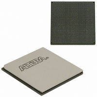
EP2SGX90EF1152C3ES Altera, EP2SGX90EF1152C3ES Datasheet - Page 134

EP2SGX90EF1152C3ES
Manufacturer Part Number
EP2SGX90EF1152C3ES
Description
IC STRATIX II GX 90K 1152-FBGA
Manufacturer
Altera
Series
Stratix® II GXr
Datasheet
1.EP2SGX30DF780C5.pdf
(316 pages)
Specifications of EP2SGX90EF1152C3ES
Number Of Logic Elements/cells
90960
Number Of Labs/clbs
4548
Total Ram Bits
4520448
Number Of I /o
558
Voltage - Supply
1.15 V ~ 1.25 V
Mounting Type
Surface Mount
Operating Temperature
0°C ~ 70°C
Package / Case
1152-FBGA
For Use With
544-1725 - PCIE KIT W/S II GX EP2SGX90N544-1724 - SI KIT W/SII GX EP2SGX90N544-1702 - VIDEO KIT W/SII GX EP2SGX90N
Lead Free Status / RoHS Status
Contains lead / RoHS non-compliant
Number Of Gates
-
Other names
544-1763
Available stocks
Company
Part Number
Manufacturer
Quantity
Price
- Current page: 134 of 316
- Download datasheet (2Mb)
I/O Structure
2–126
Stratix II GX Device Handbook, Volume 1
f
The bus-hold circuitry also pulls undriven pins away from the input
threshold voltage where noise can cause unintended high-frequency
switching. You can select this feature individually for each I/O pin. The
bus-hold output drives no higher than V
signals. If the bus-hold feature is enabled, the programmable pull-up
option cannot be used. Disable the bus-hold feature when the I/O pin has
been configured for differential signals.
The bus-hold circuitry uses a resistor with a nominal resistance (RBH) of
approximately 7 kΩ to pull the signal level to the last-driven state.
Refer to the
Stratix II GX Device Handbook for the specific sustaining current driven
through this resistor and overdrive current used to identify the
next-driven input level. This information is provided for each V
voltage level.
The bus-hold circuitry is active only after configuration. When going into
user mode, the bus-hold circuit captures the value on the pin present at
the end of configuration.
Programmable Pull-Up Resistor
Each Stratix II GX device I/O pin provides an optional programmable
pull-up resistor during user mode. If you enable this feature for an I/O
pin, the pull-up resistor (typically 25 kΩ ) holds the output to the V
level of the output pin’s bank.
Programmable pull-up resistors are only supported on user I/O pins and
are not supported on dedicated configuration pins, JTAG pins, or
dedicated clock pins.
Advanced I/O Standard Support
The Stratix II GX device IOEs support the following I/O standards:
■
■
■
■
■
■
■
■
■
■
■
3.3-V LVTTL/LVCMOS
2.5-V LVTTL/LVCMOS
1.8-V LVTTL/LVCMOS
1.5-V LVCMOS
3.3-V PCI
3.3-V PCI-X mode 1
LVDS
LVPECL (on input and output clocks only)
Differential 1.5-V HSTL class I and II
Differential 1.8-V HSTL class I and II
Differential SSTL-18 class I and II
DC & Switching Characteristics
CCIO
chapter in volume 1 of the
to prevent overdriving
Altera Corporation
October 2007
CCIO
CCIO
Related parts for EP2SGX90EF1152C3ES
Image
Part Number
Description
Manufacturer
Datasheet
Request
R

Part Number:
Description:
CYCLONE II STARTER KIT EP2C20N
Manufacturer:
Altera
Datasheet:

Part Number:
Description:
CPLD, EP610 Family, ECMOS Process, 300 Gates, 16 Macro Cells, 16 Reg., 16 User I/Os, 5V Supply, 35 Speed Grade, 24DIP
Manufacturer:
Altera Corporation
Datasheet:

Part Number:
Description:
CPLD, EP610 Family, ECMOS Process, 300 Gates, 16 Macro Cells, 16 Reg., 16 User I/Os, 5V Supply, 15 Speed Grade, 24DIP
Manufacturer:
Altera Corporation
Datasheet:

Part Number:
Description:
Manufacturer:
Altera Corporation
Datasheet:

Part Number:
Description:
CPLD, EP610 Family, ECMOS Process, 300 Gates, 16 Macro Cells, 16 Reg., 16 User I/Os, 5V Supply, 30 Speed Grade, 24DIP
Manufacturer:
Altera Corporation
Datasheet:

Part Number:
Description:
High-performance, low-power erasable programmable logic devices with 8 macrocells, 10ns
Manufacturer:
Altera Corporation
Datasheet:

Part Number:
Description:
High-performance, low-power erasable programmable logic devices with 8 macrocells, 7ns
Manufacturer:
Altera Corporation
Datasheet:

Part Number:
Description:
Classic EPLD
Manufacturer:
Altera Corporation
Datasheet:

Part Number:
Description:
High-performance, low-power erasable programmable logic devices with 8 macrocells, 10ns
Manufacturer:
Altera Corporation
Datasheet:

Part Number:
Description:
Manufacturer:
Altera Corporation
Datasheet:

Part Number:
Description:
Manufacturer:
Altera Corporation
Datasheet:

Part Number:
Description:
Manufacturer:
Altera Corporation
Datasheet:

Part Number:
Description:
CPLD, EP610 Family, ECMOS Process, 300 Gates, 16 Macro Cells, 16 Reg., 16 User I/Os, 5V Supply, 25 Speed Grade, 24DIP
Manufacturer:
Altera Corporation
Datasheet:


