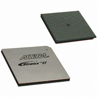
EP2S130F1508C5 Altera, EP2S130F1508C5 Datasheet - Page 228

EP2S130F1508C5
Manufacturer Part Number
EP2S130F1508C5
Description
IC STRATIX II FPGA 130K 1508FBGA
Manufacturer
Altera
Series
Stratix® IIr
Datasheet
1.EP2S15F484I4N.pdf
(238 pages)
Specifications of EP2S130F1508C5
Number Of Logic Elements/cells
132540
Number Of Labs/clbs
6627
Total Ram Bits
6747840
Number Of I /o
1126
Voltage - Supply
1.15 V ~ 1.25 V
Mounting Type
Surface Mount
Operating Temperature
0°C ~ 85°C
Package / Case
1508-FBGA
Family Name
Stratix II
Number Of Logic Blocks/elements
132540
# I/os (max)
1126
Frequency (max)
609.76MHz
Process Technology
90nm (CMOS)
Operating Supply Voltage (typ)
1.2V
Logic Cells
132540
Ram Bits
6747840
Operating Supply Voltage (min)
1.15V
Operating Supply Voltage (max)
1.25V
Operating Temp Range
0C to 85C
Operating Temperature Classification
Commercial
Mounting
Surface Mount
Pin Count
1508
Package Type
FC-FBGA
Lead Free Status / RoHS Status
Contains lead / RoHS non-compliant
Number Of Gates
-
Lead Free Status / Rohs Status
Not Compliant
Other names
544-1414
Available stocks
Company
Part Number
Manufacturer
Quantity
Price
Company:
Part Number:
EP2S130F1508C5
Manufacturer:
Altera30
Quantity:
178
Part Number:
EP2S130F1508C5
Manufacturer:
ALTERA/阿尔特拉
Quantity:
20 000
Company:
Part Number:
EP2S130F1508C5N
Manufacturer:
ALTERA
Quantity:
3 000
Part Number:
EP2S130F1508C5N
Manufacturer:
ALTERA/阿尔特拉
Quantity:
20 000
PLL Timing Specifications
5–92
Stratix II Device Handbook, Volume 1
Notes to
(1)
(2)
t
t
f
f
f
f
% spread
t
t
t
L O C K
D L O C K
S W I T C H OV E R
C L B W
V C O
S S
P L L _ P S E R R
A R E S E T
A R E S E T _ R E C O N F I G
Table 5–92. Enhanced PLL Specifications (Part 2 of 2)
Limited by I/O f
If the counter cascading feature of the PLL is utilized, there is no minimum output clock frequency.
Name
Table
5–92:
M A X
Time required for the
PLL to lock from the
time it is enabled or
the end of device
configuration
Time required for the
PLL to lock
dynamically after
automatic clock
switchover between
two identical clock
frequencies
Frequency range
where the clock
switchover performs
properly
PLL closed-loop
bandwidth
PLL VCO operating
range for –3 and –4
speed grade devices
PLL VCO operating
range for –5 speed
grade devices
Spread-spectrum
modulation frequency
Percent down spread
for a given clock
frequency
Accuracy of PLL
phase shift
Minimum pulse width
on
Minimum pulse width
on the
when using PLL
reconfiguration. Reset
the PLL after
scandone
high.
. See
areset
Description
areset
Table 5–78 on page 5–69
goes
signal.
signal
0.13
Min
300
300
500
0.4
30
10
4
for the maximum. Cannot exceed f
0.03
1.20
Typ
0.5
16.90
1,040
Max
±15
500
840
150
0.6
1
1
O U T
specification.
Altera Corporation
April 2011
MHz
MHz
MHz
MHz
Unit
kHz
ms
ms
ps
ns
ns
%


