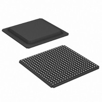
XA3S400A-4FGG400Q Xilinx Inc, XA3S400A-4FGG400Q Datasheet - Page 45

XA3S400A-4FGG400Q
Manufacturer Part Number
XA3S400A-4FGG400Q
Description
IC FPGA SPARTAN-3A 400K 400-FBGA
Manufacturer
Xilinx Inc
Series
Spartan™-3A XAr
Datasheet
1.XA3S200A-4FTG256I.pdf
(56 pages)
Specifications of XA3S400A-4FGG400Q
Number Of Logic Elements/cells
8064
Number Of Labs/clbs
896
Total Ram Bits
368640
Number Of I /o
311
Number Of Gates
400000
Voltage - Supply
1.14 V ~ 1.26 V
Mounting Type
Surface Mount
Operating Temperature
-40°C ~ 125°C
Package / Case
400-BGA
Lead Free Status / RoHS Status
Lead free / RoHS Compliant
Available stocks
Company
Part Number
Manufacturer
Quantity
Price
Company:
Part Number:
XA3S400A-4FGG400Q
Manufacturer:
XilinxInc
Quantity:
3 000
Company:
Part Number:
XA3S400A-4FGG400Q
Manufacturer:
Xilinx Inc
Quantity:
10 000
Part Number:
XA3S400A-4FGG400Q
Manufacturer:
XILINX/赛灵思
Quantity:
20 000
Configuration and JTAG Timing
General Configuration Power-On/Reconfigure Timing
Table 44: Power-On Timing and the Beginning of Configuration
DS681 (v1.1) February 3, 2009
Product Specification
Notes:
1.
2.
3.
T
T
T
T
T
POR
PROG
PL
INIT
ICCK
(2)
The numbers in this table are based on the operating conditions set forth in
and V
Power-on reset and the clearing of configuration memory occurs during this period.
This specification applies only to the Master Serial, SPI, and BPI modes.
(2)
(3)
Symbol
Notes:
1.
2.
3.
V
CCAUX
(Open-Drain)
CCO
R
PROG_B
The V
The Low-going pulse on PROG_B is optional after power-on.
The rising edge of INIT_B samples the voltage levels applied to the mode pins (M0 - M2).
(Supply)
V
(Supply)
(Supply)
V
(Output)
Bank 2
CCAUX
(Input)
INIT_B
lines.
CCINT
CCLK
CCINT
The time from the application of V
Bank 2 supply voltage ramps (whichever occurs last) to the
rising transition of the INIT_B pin
The width of the low-going pulse on the PROG_B pin
The time from the rising edge of the PROG_B pin to the
rising transition on the INIT_B pin
Minimum Low pulse width on INIT_B output
The time from the rising edge of the INIT_B pin to the
generation of the configuration clock signal at the CCLK
output pin
, V
Figure 10: Waveforms for Power-On and the Beginning of Configuration
CCAUX
, and V
CCO
supplies can be applied in any order.
1.0V
2.0V
1.0V
Description
CCINT
T
T
POR
www.xilinx.com
PROG
, V
CCAUX
, and V
T
Table
PL
CCO
8. This means power must be applied to all V
All
All
XA3S200A
XA3S400A
XA3S700A
XA3S1400A
All
All
T
Device
ICCK
-4 Speed Grade
Min
250
0.5
0.5
–
–
–
–
–
DS529-3_01_112906
Max
0.5
18
1
2
2
–
4
-
1.2V
3.3V
2.5V
or
CCINT
Units
ms
ms
ms
ms
ms
, V
μs
ns
μs
CCO
45
,


