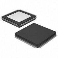
XC5206-5PQ208C Xilinx Inc, XC5206-5PQ208C Datasheet - Page 3

XC5206-5PQ208C
Manufacturer Part Number
XC5206-5PQ208C
Description
IC FPGA 196 CLB'S 208-PQFP
Manufacturer
Xilinx Inc
Series
XC5200r
Datasheet
1.XC5206-5PQ208C.pdf
(73 pages)
Specifications of XC5206-5PQ208C
Number Of Logic Elements/cells
784
Number Of Labs/clbs
196
Number Of I /o
148
Number Of Gates
10000
Voltage - Supply
4.75 V ~ 5.25 V
Mounting Type
Surface Mount
Operating Temperature
0°C ~ 85°C
Package / Case
208-BFQFP
Lead Free Status / RoHS Status
Contains lead / RoHS non-compliant
Total Ram Bits
-
Other names
122-1142
Available stocks
Company
Part Number
Manufacturer
Quantity
Price
Company:
Part Number:
XC5206-5PQ208C
Manufacturer:
XILINX
Quantity:
688
Company:
Part Number:
XC5206-5PQ208C
Manufacturer:
XILINX
Quantity:
748
XC3000 family: XC5200 devices support an additional pro-
gramming mode: Peripheral Synchronous.
XC3000 family: The XC5200 family does not support
Power-down, but offers a Global 3-state input that does not
reset any flip-flops.
XC3000 family: The XC5200 family does not provide an
on-chip crystal oscillator amplifier, but it does provide an
internal oscillator from which a variety of frequencies up to
12 MHz are available.
Architectural Overview
Figure 1
XC5200 architecture. Similar to conventional FPGAs, the
XC5200 family consists of programmable IOBs, program-
mable logic blocks, and programmable interconnect. Unlike
other FPGAs, however, the logic and local routing
resources of the XC5200 family are combined in flexible
VersaBlocks
to the VersaBlock through the General Routing Matrix
(GRM).
VersaBlock: Abundant Local Routing Plus
Versatile Logic
The basic logic element in each VersaBlock structure is the
Logic Cell, shown in
function generator (F), a storage device (FD), and control
logic. There are five independent inputs and three outputs
to each LC. The independence of the inputs and outputs
allows the software to maximize the resource utilization
within each LC. Each Logic Cell also contains a direct
feedthrough path that does not sacrifice the use of either
the function generator or the register; this feature is a first
for FPGAs. The storage device is configurable as either a D
flip-flop or a latch. The control logic consists of carry logic
for fast implementation of arithmetic functions, which can
also be configured as a cascade chain allowing decode of
very wide input functions.
November 5, 1998 (Version 5.2)
presents a simplified, conceptual overview of the
(Figure
R
2). General-purpose routing connects
Figure
Product Obsolete or Under Obsolescence
3. Each LC contains a 4-input
XC5200 Series Field Programmable Gate Arrays
Figure 1: XC5200 Architectural Overview
Figure 2: VersaBlock
Figure 3: XC5200 Logic Cell (Four LCs per CLB)
DI
F4
F3
F2
F1
Input/Output Blocks (IOBs)
F
GRM
GRM
GRM
GRM
Versa-
Versa-
Versa-
Block
Block
Block
4
4
CO
CI
24
24
TS
Direct Connects
GRM
GRM
GRM
VersaRing
VersaRing
CLB
LC3
LC2
LC1
LC0
Versa-
Versa-
Versa-
Block
Block
Block
4
4
4
4
4
CE CK
LIM
GRM
GRM
GRM
Versa-
Versa-
Versa-
Block
Block
Block
4
4
X5707
CLR
D
FD
X4955
DO
X4956
Q
X
7-85
7


