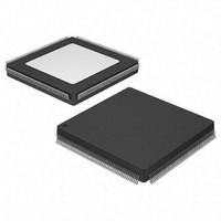
XC5206-5PQ208C Xilinx Inc, XC5206-5PQ208C Datasheet - Page 39

XC5206-5PQ208C
Manufacturer Part Number
XC5206-5PQ208C
Description
IC FPGA 196 CLB'S 208-PQFP
Manufacturer
Xilinx Inc
Series
XC5200r
Datasheet
1.XC5206-5PQ208C.pdf
(73 pages)
Specifications of XC5206-5PQ208C
Number Of Logic Elements/cells
784
Number Of Labs/clbs
196
Number Of I /o
148
Number Of Gates
10000
Voltage - Supply
4.75 V ~ 5.25 V
Mounting Type
Surface Mount
Operating Temperature
0°C ~ 85°C
Package / Case
208-BFQFP
Lead Free Status / RoHS Status
Contains lead / RoHS non-compliant
Total Ram Bits
-
Other names
122-1142
Available stocks
Company
Part Number
Manufacturer
Quantity
Price
Company:
Part Number:
XC5206-5PQ208C
Manufacturer:
XILINX
Quantity:
688
Company:
Part Number:
XC5206-5PQ208C
Manufacturer:
XILINX
Quantity:
748
Notes: 1. Configuration must be delayed until INIT pins of all daisy-chained FPGAs are high.
This timing diagram shows very relaxed requirements. Data need not be held beyond the rising edge of WS. RDY/BUSY will
go active within 60 ns after the end of WS. A new write may be asserted immediately after RDY/BUSY goes Low, but write
may not be terminated until RDY/BUSY has been High for one CCLK period.
Figure 36: Asynchronous Peripheral Mode Programming Switching Characteristics
November 5, 1998 (Version 5.2)
RDY/BUSY
WS/CS0
RS, CS1
D0-D7
DOUT
CCLK
Write
2. The time from the end of WS to CCLK cycle for the new byte of data depends on the completion of previous byte processing
3. CCLK and DOUT timing is tested in slave mode.
4. T
RDY
and the phase of internal timing generator for CCLK.
occurs when a byte is loaded into an empty parallel-to-serial converter. The longest T
loaded into the input register before the second-level buffer has started shifting out data.
BUSY
R
indicates that the double-buffered parallel-to-serial converter is not yet ready to receive new data. The shortest T
Effective Write time
(CSO, WS=Low; RS, CS1=High
DIN setup time
DIN hold time
RDY/BUSY delay after end of
RDY/BUSY active after beginning
Write or Read
of Read
RDY/BUSY Low output (Note 4)
Product Obsolete or Under Obsolescence
Write to LCA
1 T
T
CA
WTRB
Description
2 T
DC
4
Previous Byte D6
3 T
CD
XC5200 Series Field Programmable Gate Arrays
1
2
3
4
7
6
6 T
Symbol
BUSY
T
T
T
T
T
WTRB
BUSY
DC
CD
CA
D7
7
Min
100
60
0
2
BUSY
D0
Read Status
occurs when a new word is
READY
BUSY
D1
Max
60
60
9
4
D2
periods
CCLK
Units
BUSY
RS, CS0
WS, CS1
D7
ns
ns
ns
ns
ns
X6097
7-121
7


