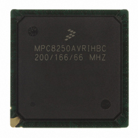
MPC8250AVRIHBC Freescale Semiconductor, MPC8250AVRIHBC Datasheet - Page 20

MPC8250AVRIHBC
Manufacturer Part Number
MPC8250AVRIHBC
Description
IC MPU POWERQUICC II 516-PBGA
Manufacturer
Freescale Semiconductor
Datasheet
1.MPC8250AVRIHBC.pdf
(62 pages)
Specifications of MPC8250AVRIHBC
Processor Type
MPC82xx PowerQUICC II 32-bit
Speed
200MHz
Voltage
1.8V
Mounting Type
Surface Mount
Package / Case
516-PBGA
Processor Series
MPC8xxx
Core
603e
Data Bus Width
32 bit
Maximum Clock Frequency
200 MHz
Maximum Operating Temperature
+ 105 C
Mounting Style
SMD/SMT
Minimum Operating Temperature
0 C
Family Name
MPC82XX
Device Core
PowerQUICC II
Device Core Size
32b
Frequency (max)
200MHz
Instruction Set Architecture
RISC
Supply Voltage 1 (typ)
1.8V
Operating Supply Voltage (max)
1.9V
Operating Supply Voltage (min)
1.7V
Operating Temp Range
0C to 105C
Operating Temperature Classification
Commercial
Mounting
Surface Mount
Pin Count
516
Package Type
TEPBGA
Leaded Process Compatible
Yes
Rohs Compliant
Yes
Peak Reflow Compatible (260 C)
Yes
For Use With
CWH-PPC-8248N-VE - KIT EVAL SYSTEM QUICCSTART 8248
Lead Free Status / RoHS Status
Lead free / RoHS Compliant
Features
-
Lead Free Status / Rohs Status
Lead free / RoHS Compliant
Available stocks
Company
Part Number
Manufacturer
Quantity
Price
Company:
Part Number:
MPC8250AVRIHBC
Manufacturer:
MOTOLOLA
Quantity:
875
Company:
Part Number:
MPC8250AVRIHBC
Manufacturer:
Freescale Semiconductor
Quantity:
10 000
Clock Configuration Modes
3
The MPC8250 has three clocking modes: local, PCI host, and PCI agent. The clocking mode is set
according to three input pins—PCI_MODE, PCI_CFG[0], PCI_MODCK—as shown in
In each clocking mode, the configuration of bus, core, PCI, and CPM frequencies is determined by seven
bits during the power-up reset—three hardware configuration pins (MODCK[1–3]) and four bits from
hardware configuration word[28–31] (MODCK_H). Both the PLLs and the dividers are set according to
the selected MPC8250 clock operation mode as described in the following sections.
3.1
Table 13
available by using the configuration pin (RSTCONF) and driving four pins on the data bus.
20
1
PCI_MODE
Determines PCI clock frequency range. Refer to
Clock Configuration Modes
MODCK[1–3]
1
0
0
0
0
shows the eight basic clock configurations for the MPC8250. Another 49 configurations are
Local Bus Mode
000
001
010
011
The UPM machine outputs change on the internal tick determined by the
memory controller programming; the AC specifications are relative to the
internal tick. Note that SDRAM and GPCM machine outputs change on
CLKin’s rising edge.
Clock configurations change only after POR is asserted.
PCI_CFG[0] PCI_MODCK
Pins
—
0
0
1
1
Input Clock
Frequency
33 MHz
33 MHz
33 MHz
33 MHz
—
Table 13. Clock Default Configurations
0
1
0
1
MPC8250 Hardware Specifications, Rev. 2
CPM Multiplication
Table 12. MPC8250 Clocking Modes
1
Factor
3
3
4
4
Clocking Mode
Section 3.2, “PCI
PCI agent
Local bus
PCI host
NOTE
NOTE
Frequency
100 MHz
100 MHz
133 MHz
133 MHz
CPM
Mode.”
Frequency Range
Core Multiplication
PCI Clock
(MHZ)
50–66
25–50
50–66
25–50
Factor
—
4
5
4
5
Table 13
Table 15
Table 17
Freescale Semiconductor
Frequency
133 MHz
166 MHz
133 MHz
166 MHz
Reference
Table
Core
and
and
and
Table 14
Table 16
Table 18
12.


