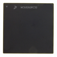
MC68060RC50 Freescale Semiconductor, MC68060RC50 Datasheet - Page 8

MC68060RC50
Manufacturer Part Number
MC68060RC50
Description
IC MPU 32BIT 50MHZ 206-PGA
Manufacturer
Freescale Semiconductor
Specifications of MC68060RC50
Processor Type
M680x0 32-Bit
Speed
50MHz
Voltage
3.3V
Mounting Type
Surface Mount
Package / Case
206-PGA
Family Name
M68000
Device Core
ColdFire
Device Core Size
32b
Frequency (max)
50MHz
Instruction Set Architecture
RISC
Supply Voltage 1 (typ)
3.3V
Operating Supply Voltage (max)
3.465V
Operating Supply Voltage (min)
3.135V
Operating Temp Range
0C to 110C
Operating Temperature Classification
Commercial
Mounting
Through Hole
Pin Count
206
Package Type
PGA
Lead Free Status / RoHS Status
Contains lead / RoHS non-compliant
Features
-
Lead Free Status / Rohs Status
Compliant
Available stocks
Company
Part Number
Manufacturer
Quantity
Price
Company:
Part Number:
MC68060RC50
Manufacturer:
MOTO
Quantity:
5 530
Company:
Part Number:
MC68060RC50C
Manufacturer:
MOTO
Quantity:
5 530
Company:
Part Number:
MC68060RC50C
Manufacturer:
MOTO
Quantity:
5 530
Company:
Part Number:
MC68060RC50C
Manufacturer:
SAMSUNG
Quantity:
5 704
Freescale Semiconductor, Inc.
CACHE ORGANIZATION
The instruction and data caches are each organized as four-way set associative, with 16-byte lines. Each line
of data has associated with it an address tag and state information that shows the line’s validity. In the data
cache, the state information indicates whether the line is invalid, valid, or dirty.
CACHE COHERENCY
The MC68060 has the ability to watch, or snoop, the external bus during accesses by other bus masters,
maintaining coherency between the MC68060 caches and external memory systems. External bus cycles can
be flagged on the bus as snoopable or nonsnoopable. When an external cycle is marked as snoopable, the
bus snooper checks the caches and invalidates the matching data. Although the execution unit and the bus
snooper circuit have access to the on-chip caches, the snooper has priority over the execution unit.
BUS CONTROLLER
The bus is implemented as a nonmultiplexed, fully synchronous protocol that is clocked off the rising edge of
the input clock. It is compatible with an MC68040 bus. The bus controller operates concurrently with all other
functional units of the MC68060 to maximize system throughput. The timing of the bus is fully configurable to
match external memory requirements.
The CLKEN input is used on the MC68060 to enable to the clock edges on which the bus controller will
respond. By toggling the CLKEN pin, it is possible to operate the MC68060 on an external bus at 1/2 or 1/4
the speed of the processor clock.
Although the MC68060 bus is compatible with the MC68040, additional signals and protocols have been
added to simplify designs requiring very high bus speeds.
IEEE 1149.1 TEST
To aid in system diagnostics, the MC68060 includes dedicated user-accessible test logic that is fully compliant
with the IEEE 1149.1 standard for boundary scan testability, often referred to as Joint Test Action Group
(JTAG).
8
MC68060 PRODUCT INFORMATION
MOTOROLA
For More Information On This Product,
Go to: www.freescale.com


