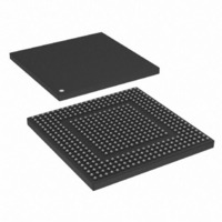
MPC8308CVMAFD Freescale Semiconductor, MPC8308CVMAFD Datasheet - Page 42

MPC8308CVMAFD
Manufacturer Part Number
MPC8308CVMAFD
Description
MPU POWERQUICC II PRO 473MAPBGA
Manufacturer
Freescale Semiconductor
Series
PowerQUICC II PROr
Datasheets
1.MPC8308VMAGD.pdf
(90 pages)
2.MPC8308VMAGD.pdf
(2 pages)
3.MPC8308VMAGD.pdf
(1170 pages)
4.MPC8308VMAGD.pdf
(14 pages)
Specifications of MPC8308CVMAFD
Processor Type
MPC83xx PowerQUICC II Pro 32-Bit
Speed
333MHz
Voltage
1V
Mounting Type
Surface Mount
Package / Case
473-MAPBGA
Product
Network Processor
Data Rate
256 bps
Frequency
333 MHz
Supply Voltage (max)
3.6 V
Supply Voltage (min)
3 V
Supply Current (max)
5 uA
Maximum Operating Temperature
+ 105 C
Minimum Operating Temperature
- 40 C
Interface
I2C, JTAG, SPI
Mounting Style
SMD/SMT
Core Size
32 Bit
Cpu Speed
333MHz
Digital Ic Case Style
MAPBGA
No. Of Pins
473
Operating Temperature Range
-40°C To +105°C
Peak Reflow Compatible (260 C)
Yes
Rohs Compliant
Yes
Leaded Process Compatible
Yes
Lead Free Status / RoHS Status
Lead free / RoHS Compliant
Features
-
Lead Free Status / Rohs Status
Lead free / RoHS Compliant
Available stocks
Company
Part Number
Manufacturer
Quantity
Price
Company:
Part Number:
MPC8308CVMAFD
Manufacturer:
Freescale Semiconductor
Quantity:
10 000
Company:
Part Number:
MPC8308CVMAFDA
Manufacturer:
Freescale Semiconductor
Quantity:
10 000
PCI Express
11.5
The RX eye diagram in
(Figure
measured with the compliance/test measurement load
diagram measured over a range of systems at the input receiver of any real PCI Express component. The
degraded eye diagram at the input Receiver is due to traces internal to the package as well as silicon
parasitic characteristics which cause the real PCI Express component to vary in impedance from the
compliance/test measurement load. The input receiver eye diagram is implementation specific and is not
specified. RX component designer should provide additional margin to adequately compensate for the
degraded minimum Receiver eye diagram (shown in
adequate combination of system simulations and the return loss measured looking into the RX package
42
Total Skew
Notes:
1. No test load is necessarily associated with this value.
2. Specified at the measurement point and measured over any 250 consecutive UIs. The test load in
3. A T
4. The receiver input impedance shall result in a differential return loss greater than or equal to 15 dB with the D+ line biased to
5. Impedance during all LTSSM states. When transitioning from a fundamental reset to detect (the initial state of the LTSSM)
6. The RX DC common mode impedance that exists when no power is present or fundamental reset is asserted. This helps
7. It is recommended that the recovered TX UI is calculated using all edges in the 3500 consecutive UI interval with a fit algorithm
as the RX device when taking measurements (also refer to the receiver compliance eye diagram shown in
clocks to the RX and TX are not derived from the same reference clock, the TX UI recovered from 3500 consecutive UI must
be used as a reference for the eye diagram.
interconnect collected any 250 consecutive UIs. The T
which the median and the maximum deviation from the median is less than half of the total. UI jitter budget collected over any
250 consecutive TX UIs. It should be noted that the median is not the same as the mean. The jitter median describes the point
in time where the number of jitter points on either side is approximately equal as opposed to the averaged time value. If the
clocks to the RX and TX are not derived from the same reference clock, the TX UI recovered from 3500 consecutive UI must
be used as the reference for the eye diagram.
300 mV and the D– line biased to –300 mV and a common mode return loss greater than or equal to 6 dB (no bias required)
over a frequency range of 50 MHz to 1.25 GHz. This input impedance requirement applies to all valid input levels. The
reference impedance for return loss measurements for is 50 Ω to ground for both the D+ and D– line (that is, as measured by
a vector network analyzer with 50-Ω probes, see
loss measurement.
there is a 5 ms transition time before receiver termination values must be met on all unconfigured lanes of a port.
ensure that the receiver detect circuit does not falsely assume a receiver is powered on when it is not. This term must be
measured at 300 mV above the RX ground.
using a minimization merit function. Least squares and median deviation fits have worked well with experimental and
simulated data.
RX-EYE
Parameter
29) in place of any real PCI Express RX component. In general, the minimum receiver eye diagram
Receiver Compliance Eye Diagrams
= 0.40 UI provides for a total sum of 0.60 UI deterministic and random jitter budget for the transmitter and
Table 35. Differential Receiver (RX) Input Specifications (continued)
MPC8308 PowerQUICC II Pro Processor Hardware Specification, Rev. 2
Figure 28
L
Symbol
RX-SKEW
is specified using the passive compliance/test measurement load
Skew across all lanes on a
Link. This includes
variation in the length of
SKP ordered set (for
example, COM and one to
five SKP Symbols) at the
RX as well as any delay
differences arising from
the interconnect itself.
Figure
Comments
RX-EYE-MEDIAN-to-MAX-JITTER
29). Note that the series capacitors, C
Figure
(Figure
28) expected at the input receiver based on an
29) is larger than the minimum receiver eye
Min
—
specification ensures a jitter distribution in
Typical
—
TX
Max
20
, is optional for the return
Figure 29
Freescale Semiconductor
Units
Figure
ns
should be used
28). If the
Notes
—


