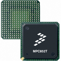
MPC852TVR100A Freescale Semiconductor, MPC852TVR100A Datasheet - Page 9

MPC852TVR100A
Manufacturer Part Number
MPC852TVR100A
Description
IC MPU POWERQUICC 100MHZ 256PBGA
Manufacturer
Freescale Semiconductor
Series
PowerQUICC Ir
Datasheet
1.MPC852TVR50A.pdf
(80 pages)
Specifications of MPC852TVR100A
Processor Type
MPC8xx PowerQUICC 32-Bit
Speed
100MHz
Voltage
1.8V
Mounting Type
Surface Mount
Package / Case
256-PBGA
Processor Series
MPC8xx
Core
MPC8xx
Data Bus Width
32 bit
Development Tools By Supplier
MPC852TADS-KIT
Maximum Clock Frequency
100 MHz
Operating Supply Voltage
0 V to 3.3 V
Maximum Operating Temperature
+ 105 C
Mounting Style
SMD/SMT
Data Ram Size
8 KB
I/o Voltage
3.3 V
Interface Type
SPI, UART
Minimum Operating Temperature
0 C
Program Memory Size
4 KB
Program Memory Type
EPROM/Flash
Core Size
32 Bit
Cpu Speed
100MHz
Embedded Interface Type
SPI, UART
Digital Ic Case Style
BGA
No. Of Pins
256
Supply Voltage Range
1.7V To 1.9V
Rohs Compliant
Yes
Lead Free Status / RoHS Status
Contains lead / RoHS non-compliant
Features
-
Lead Free Status / Rohs Status
Lead free / RoHS Compliant
Available stocks
Company
Part Number
Manufacturer
Quantity
Price
Company:
Part Number:
MPC852TVR100A
Manufacturer:
MOTOROLA
Quantity:
490
Company:
Part Number:
MPC852TVR100A
Manufacturer:
Freescale Semiconductor
Quantity:
10 000
1
2
3
4
7
For the following discussions, P
drivers.
7.1
An estimation of the chip junction temperature, T
Freescale Semiconductor
Input leakage current, Vin = 5.5 V (Except TMS, TRST,
DSCK and DSDI pins) for 5-V tolerant pins
Input leakage current, Vin = V
DSCK, and DSDI)
Input leakage current, Vin = 0 V (Except TMS, TRST,
DSCK and DSDI pins)
Input capacitance
Output high voltage, IOH = -2.0 mA, V
Except XTAL and open drain pins
Output low voltage
IOL = 2.0 mA (CLKOUT)
IOL = 3.2 mA
IOL = 5.3 mA
IOL = 7.0 mA (Txd1/pa14, txd2/pa12)
IOL = 8.9 mA (TS, TA, TEA, BI, BB, HRESET, SRESET)
The PA[0:3], PA[8:11], PB15, PB[24:25]; PB[28:31], PC[4:7], PC[12:13], PC15, PD[3:15], TDI, TDO, TCK, TRST, TMS,
MII_TXEN, MII_MDIO are 5-V tolerant pins.
Input capacitance is periodically sampled.
A(0:31), TSIZ0/REG, TSIZ1, D(0:31), DP(0:3)/IRQ(3:6), RD/WR, BURST, RSV/IRQ2, IWP(0:1)/VFLS(0:1), RXD3/PA11,
TXD3/PA10, RXD4/PA9, TXD4/PA8, TIN3/BRGO3/CLK5/PA3, BRGCLK2/TOUT3/CLK6/PA2, TIN4/BRGO4/CLK7/PA1,
TOUT4/CLK8/PA0, SPISEL/PB31, SPICLK/PB30, SPIMOSI/PB29, BRGO4/SPIMISO/PB28, SMTXD1/PB25,
SMRXD1/PB24, BRGO3/PB15, RTS1/DREQ0/PC15, RTS3/PC13, RTS4/PC12, CTS3/PC7, CD3/PC6, CTS4/SDACK1/PC5,
CD4/PC4, MII-RXD3/PD15, MII-RXD2/PD14, MII-RXD1/PD13, MII-MDC/PD12, MII-TXERR/RXD3/PD11,
MII-RX0/TXD3/PD10, MII-TXD0/RXD4/PD9, MII-RXCLK/TXD4/PD8, MII-TXD3/PD5, MII-RXDV/RTS4/PD6,
MII-RXERR/RTS3/PD7, MII-TXD2/REJECT3/PD4, MII-TXD1/REJECT4/PD3, MII_CRS, MII_MDIO, MII_TXEN, and MII_COL
BDIP/GPL_B(5), BR, BG, FRZ/IRQ6, CS(0:5), CS(6), CS(7), WE0/BS_B0/IORD, WE1/BS_B1/IOWR, WE2/BS_B2/PCOE,
WE3/ BS_B3/PCWE, BS_A(0:3), GPL_A0/GPL_B0, OE/GPL_A1/GPL_B1, GPL_A(2:3)/GPL_B(2:3)/CS(2:3),
UPWAITA/GPL_A4, GPL_A5, ALE_A, CE1_A, CE2_A, DSCK, OP(0:1), OP2/MODCK1/STS, OP3/MODCK2/DSDO, and
BADDR(28:30)
Thermal Calculation and Measurement
Estimation with Junction-to-Ambient Thermal Resistance
3
4
T
2
J
= T
Characteristic
A
+(R
DDH
θJA
MPC852T PowerQUICC™ Hardware Specifications, Rev. 4
Table 5. DC Electrical Specifications (continued)
(Except TMS, TRST,
The V
× P
D
DDH
= (V
D
)
= 3.0 V
1
DDSYN
DDL
x IDDL) + P
power dissipation is negligible.
J
NOTE
, in °C can be obtained from the equation:
Symbol
I/O
VOH
VOL
C
I
I
I
, where P
in
In
In
in
I/O
is the power dissipation of the I/O
Min
Thermal Calculation and Measurement
2.4
—
—
—
—
—
Max
100
0.5
10
10
20
—
Unit
µA
µA
µA
pF
V
V
9


