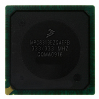
MPC8313EZQAFFB Freescale Semiconductor, MPC8313EZQAFFB Datasheet - Page 10

MPC8313EZQAFFB
Manufacturer Part Number
MPC8313EZQAFFB
Description
IC MPU POWERQUICC II PRO 516PBGA
Manufacturer
Freescale Semiconductor
Datasheet
1.MPC8313CZQAFFB.pdf
(100 pages)
Specifications of MPC8313EZQAFFB
Processor Type
MPC83xx PowerQUICC II Pro 32-Bit
Speed
333MHz
Voltage
0.95 V ~ 1.05 V
Mounting Type
Surface Mount
Package / Case
516-PBGA
Processor Series
MPC8xxx
Core
e300
Data Bus Width
32 bit
Development Tools By Supplier
MPC8313E-RDB
Maximum Clock Frequency
333 MHz
Operating Supply Voltage
1 V, 3.3 V
Maximum Operating Temperature
+ 105 C
Mounting Style
SMD/SMT
I/o Voltage
1 V, 1.8 V, 2.5 V, 3.3 V
Minimum Operating Temperature
0 C
For Use With
MPC8313E-RDB - BOARD PROCESSOR
Lead Free Status / RoHS Status
Lead free / RoHS Compliant
Features
-
Lead Free Status / Rohs Status
Lead free / RoHS Compliant
Available stocks
Company
Part Number
Manufacturer
Quantity
Price
Company:
Part Number:
MPC8313EZQAFFB
Manufacturer:
Freescale Semiconductor
Quantity:
10 000
Power Characteristics
and V
supplies fully ramp up. In the case where the core voltage is applied first, the core voltage supply must rise
to 90% of its nominal value before the I/O supplies reach 0.7 V; see
(I/O voltage and core voltage) are stable, wait for a minimum of 32 clock cycles before negating
PORESET.
Note that there is no specific power down sequence requirement for the MPC8313E. I/O voltage supplies
(GV
3
The estimated typical power dissipation, not including I/O supply power, for this family of MPC8313E
devices is shown in
10
DD
DDC
, LV
Power Characteristics
1
2
3
Core Frequency
The values do not include I/O supply power or AV
digital power (not including XCOREV
the SerDes PHY).
Typical power is based on a voltage of V
temperature.
Maximum power is based on a voltage of V
smoker test.
) before the I/O voltage (GV
DD
(MHz)
, and OV
333
400
90%
MPC8313E PowerQUICC
Table
V
0
DD
PORESET
4.
) do not have any ordering requirements with respect to one another.
CSB Frequency
Table 5
(MHz)
Figure 3. Power-Up Sequencing Example
167
133
Table 4. MPC8313E Power Dissipation
shows the estimated typical I/O power dissipation.
DD
DD
™
, LV
, XPADV
II Pro Processor Hardware Specifications, Rev. 3
DD
DD
= 1.05 V and an artificial smoker test running at room
Typical
DD
= 1.05 V, a junction temperature of T
820
820
DD
, and OV
DD
, or SDAV
, but do include core, USB PLL, and a portion of SerDes
2
I/O Voltage (GV
t
SYS_CLK_IN
Maximum for
DD
DD
Silicon
Rev. 1.0
, which all have dedicated power supplies for
) and assert PORESET before the power
1020
1020
Core Voltage (V
/t
3
PCI_SYNC_IN
Figure
DD
, GV
1
Rev. 2.x or Later
3. Once both the power supplies
Maximum for
DD
DD
, and OV
Silicon
J
>= 32 clocks
= 105°C, and an artificial
1200
1200
, V
0.7 V
DDC
3
)
DD
Freescale Semiconductor
)
t
Unit
mW
mW


