MPC8347VRADDB Freescale Semiconductor, MPC8347VRADDB Datasheet - Page 18
MPC8347VRADDB
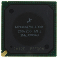
Manufacturer Part Number
MPC8347VRADDB
Description
IC MPU POWERQUICC II 620-PBGA
Manufacturer
Freescale Semiconductor
Series
PowerQUICC II PROr
Specifications of MPC8347VRADDB
Processor Type
MPC83xx PowerQUICC II Pro 32-Bit
Speed
266MHz
Voltage
1.2V
Mounting Type
Surface Mount
Package / Case
620-PBGA
Processor Series
MPC8xxx
Core
e300
Data Bus Width
32 bit
Development Tools By Supplier
MPC8349E-MITXE
Maximum Clock Frequency
266 MHz
Maximum Operating Temperature
+ 105 C
Mounting Style
SMD/SMT
I/o Voltage
1.8 V, 2.5 V, 3.3 V
Minimum Operating Temperature
0 C
Core Size
32 Bit
Program Memory Size
64KB
Cpu Speed
266MHz
Embedded Interface Type
I2C, SPI, USB, UART
Digital Ic Case Style
BGA
No. Of Pins
672
Rohs Compliant
Yes
Lead Free Status / RoHS Status
Lead free / RoHS Compliant
Features
-
Lead Free Status / Rohs Status
Lead free / RoHS Compliant
Available stocks
Company
Part Number
Manufacturer
Quantity
Price
Company:

Part Number:
MPC8347VRADDB
Manufacturer:
Freescale Semiconductor
Quantity:
135
Company:
Part Number:
MPC8347VRADDB
Manufacturer:
Freescale Semiconductor
Quantity:
10 000


DDR SDRAM
Figure 5
Figure 6
18
At recommended operating conditions with GV
MDQS epilogue end
Notes:
1. The symbols used for timing specifications follow the pattern of t
2. All MCK/MCK referenced measurements are made from the crossing of the two signals ±0.1 V.
3. In the source synchronous mode, MCK/MCK can be shifted in 1/4 applied cycle increments through the clock control register.
4. ADDR/CMD includes all DDR SDRAM output signals except MCK/MCK, MCS, and MDQ/MECC/MDM/MDQS. For the
5. Note that t
6. Determined by maximum possible skew between a data strobe (MDQS) and any corresponding bit of data (MDQ), ECC
7. All outputs are referenced to the rising edge of MCK(n) at the pins of the MPC8347E. Note that t
inputs and t
(DD) from the rising or falling edge of the reference clock (KH or KL) until the output went invalid (AX or DX). For example,
t
(A) are setup (S) or output valid time. Also, t
(K) goes low (L) until data outputs (D) are invalid (X) or data output hold time.
For the skew measurements referenced for t
address/command valid with the rising edge of MCK.
ADDR/CMD setup and hold specifications, it is assumed that the clock control register is set to adjust the memory clocks by
1/2 applied cycle.
from the rising edge of the MCK(n) clock (KH) until the MDQS signal is valid (MH). t
of the DQSS override bits in the TIMING_CFG_2 register. In source synchronous mode, this will typically be set to the same
delay as the clock adjust in the CLK_CNTL register. The timing parameters listed in the table assume that these 2 parameters
have been set to the same adjustment value. See the MPC8349E PowerQUICC™ II Pro Integrated Host Processor Family
Reference Manual , for a description and understanding of the timing modifications enabled by use of these bits.
(MECC), or data mask (MDM). The data strobe should be centered inside of the data eye at the pins of the MPC8347E.
conventions described in note 1.
DDKHAS
Table 14. DDR SDRAM Output AC Timing Specifications for Source Synchronous Mode (continued)
shows the DDR SDRAM output timing for address skew with respect to any MCK.
provides the AC test load for the DDR bus.
symbolizes DDR timing (DD) for the time t
DDKHMH
MPC8347E PowerQUICC™ II Pro Integrated Host Processor Hardware Specifications, Rev. 11
(first two letters of functional block)(reference)(state)(signal)(state)
Parameter
follows the symbol conventions described in note 1. For example, t
Figure 5. Timing Diagram for t
ADDR/CMD
ADDR/CMD
MCK[n]
MCK[n]
DD
of 2.5 V ± 5%.
DDKLDX
AOSKEW
Symbol
t
DDKLME
MCK
symbolizes DDR timing (DD) for the time t
it is assumed that the clock adjustment is set to align the
memory clock reference (K) goes from the high (H) state until outputs
1
t
CMD
AOSKEW(min)
t
AOSKEWmax)
CMD
t
(first two letters of functional block)(signal)(state)(reference)(state)
MCK
for outputs. Output hold time can be read as DDR timing
AOSKEW
Min
-0.9
NOOP
Measurement
NOOP
DDKHMH
DDKHMH
Max
0.3
can be modified through control
describes the DDR timing (DD)
MCK
DDKHMP
Freescale Semiconductor
memory clock reference
follows the symbol
Unit
ns
Notes
for
7
Related parts for MPC8347VRADDB
Image
Part Number
Description
Manufacturer
Datasheet
Request
R

Part Number:
Description:
Integrated Host Processor Hardware Specifications
Manufacturer:
FREESCALE [Freescale Semiconductor, Inc]
Datasheet:

Part Number:
Description:
Manufacturer:
Freescale Semiconductor, Inc
Datasheet:
Part Number:
Description:
Manufacturer:
Freescale Semiconductor, Inc
Datasheet:
Part Number:
Description:
Manufacturer:
Freescale Semiconductor, Inc
Datasheet:
Part Number:
Description:
Manufacturer:
Freescale Semiconductor, Inc
Datasheet:
Part Number:
Description:
Manufacturer:
Freescale Semiconductor, Inc
Datasheet:
Part Number:
Description:
Manufacturer:
Freescale Semiconductor, Inc
Datasheet:
Part Number:
Description:
Manufacturer:
Freescale Semiconductor, Inc
Datasheet:
Part Number:
Description:
Manufacturer:
Freescale Semiconductor, Inc
Datasheet:
Part Number:
Description:
Manufacturer:
Freescale Semiconductor, Inc
Datasheet:
Part Number:
Description:
Manufacturer:
Freescale Semiconductor, Inc
Datasheet:
Part Number:
Description:
Manufacturer:
Freescale Semiconductor, Inc
Datasheet:
Part Number:
Description:
Manufacturer:
Freescale Semiconductor, Inc
Datasheet:
Part Number:
Description:
Manufacturer:
Freescale Semiconductor, Inc
Datasheet:
Part Number:
Description:
Manufacturer:
Freescale Semiconductor, Inc
Datasheet: