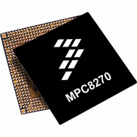
MPC8270ZQMIBA Freescale Semiconductor, MPC8270ZQMIBA Datasheet - Page 56

MPC8270ZQMIBA
Manufacturer Part Number
MPC8270ZQMIBA
Description
IC MPU POWERQUICC II 516-PBGA
Manufacturer
Freescale Semiconductor
Series
PowerQUICC IIr
Datasheet
1.MPC8270VRMIBA.pdf
(80 pages)
Specifications of MPC8270ZQMIBA
Processor Type
MPC82xx PowerQUICC II 32-bit
Speed
333MHz
Voltage
1.5V
Mounting Type
Surface Mount
Package / Case
516-PBGA
Family Name
MPC82XX
Device Core
PowerQUICC II
Device Core Size
32b
Frequency (max)
266MHz
Instruction Set Architecture
RISC
Operating Supply Voltage (max)
1.6V
Operating Supply Voltage (min)
1.45V
Operating Temp Range
0C to 105C
Operating Temperature Classification
Commercial
Mounting
Surface Mount
Pin Count
516
Package Type
FBGA
Core Size
32 Bit
Program Memory Size
32KB
Cpu Speed
266MHz
Embedded Interface Type
Ethernet, I2C, SPI, USB
Digital Ic Case Style
BGA
No. Of Pins
516
Rohs Compliant
No
Lead Free Status / RoHS Status
Contains lead / RoHS non-compliant
Features
-
Lead Free Status / Rohs Status
Not Compliant
Available stocks
Company
Part Number
Manufacturer
Quantity
Price
Company:
Part Number:
MPC8270ZQMIBA
Manufacturer:
MOTOLOLA
Quantity:
745
Company:
Part Number:
MPC8270ZQMIBA
Manufacturer:
Freescale Semiconductor
Quantity:
10 000
Part Number:
MPC8270ZQMIBA
Manufacturer:
FREESCALE
Quantity:
20 000
Company:
Part Number:
MPC8270ZQMIBA266/200/66
Manufacturer:
FREESCAL
Quantity:
850
Pinout
Symbols used in
56
1
2
3
4
5
6
7
PCI_MODE
SPARE6
No connect
I/O power
Core power
Ground
OVERBAR
UTM
UTS
DC current, it is recommended to either pull unused pins to GND or VDDH, or to configure them as outputs.
ground signal on the MPC8280. New designs must connect AB1 to GND and follow the suggestions in
“Layout
to GND with the noise filtering capacitors.
external capacitor to operate the PLL. New designs should connect AB2 (XFC) pin to GND. Old designs in which the
MPC8280 is used as a drop-in replacement can leave the pin connected to the current capacitor.
Should be tied to VDDH via a 2K Ω external pull-up resistor.
The default configuration of the CPM pins (PA[0–31], PB[4–31], PC[0–31], PD[4–31]) is input. To prevent excessive
Must be pulled down or left floating.
If PCI is not desired, must be pulled up or left floating.
Sphere is not connected to die.
GNDSYN (AB1): This pin exists as a separate ground signal in MPC826x(A) devices; it does not exist as a separate
XFC (AB2) pin: This pin is used in MPC826x(A) devices; it is not used in MPC8280 because there is no need for
Symbol
3
MPC8280/MPC8270
Practices.” Old designs in which the MPC8280 is used as a drop-in replacement can leave the pin connected
Table 21. MPC8280 and MPC8270 (ZU and VV Packages) Pinout List (continued)
5
4
Table 21
MPC8280 PowerQUICC™ II Family Hardware Specifications, Rev. 1.8
Signals with overbars, such as TA, are active low.
Indicates that a signal is part of the UTOPIA master interface.
Indicates that a signal is part of the UTOPIA slave interface.
are described in
Pin Name
Table
Table 22. Symbol Legend
22.
MPC8280 only
Meaning
AG21, AG14, AG8, AJ1, AJ2,
AH1, AH2, AG3, AF4, AE5, AC27,
Y27, T27, P27, K26, G27, AE25,
AF26, AG27, AH28, AH29, AJ28,
AJ29, C7, C14, C16, C20, C23,
E10, A28, A29, B28, B29, C27,
D26, E25, H3, M4, T3, AA4, A1,
A2, B1, B2, C3, D4, E5
U28, U29, K28, K29, A9, A19,
B19, M1, M2, Y1, Y2, AC1, AC2,
AH19, AJ19, AH10, AJ10, AJ5
AA5, AB1
AF8, AE7, AF11, AE17, AE23,
AC26, AB25, Y26, V25, T26, R25,
P26, M25, K27, H25, G26, D7,
D10, D14, D16, D20, D23, C9,
E11, E13, E15, E19, E22, B3, G5,
H4, K5, M3, P5, T4, Y5, AA2, AC3
6
, AB2
AA1, AG4
Freescale Semiconductor
AF25
Ball
V4
7
, AF21, AF14,
Section 4.6,


