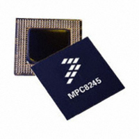
MPC8245ARVV400D Freescale Semiconductor, MPC8245ARVV400D Datasheet - Page 46

MPC8245ARVV400D
Manufacturer Part Number
MPC8245ARVV400D
Description
IC MPU 32BIT 400MHZ 352-TBGA
Manufacturer
Freescale Semiconductor
Datasheet
1.MPC8245LZU266D.pdf
(68 pages)
Specifications of MPC8245ARVV400D
Processor Type
MPC82xx PowerQUICC II 32-bit
Speed
400MHz
Voltage
2.1V
Mounting Type
Surface Mount
Package / Case
352-TBGA
Processor Series
MPC8xxx
Core
603e
Data Bus Width
32 bit
Maximum Clock Frequency
400 MHz
Maximum Operating Temperature
+ 105 C
Mounting Style
SMD/SMT
Minimum Operating Temperature
0 C
Lead Free Status / RoHS Status
Lead free / RoHS Compliant
Features
-
Lead Free Status / Rohs Status
Lead free / RoHS Compliant
Available stocks
Company
Part Number
Manufacturer
Quantity
Price
Company:
Part Number:
MPC8245ARVV400D
Manufacturer:
Freescale Semiconductor
Quantity:
162 528
Company:
Part Number:
MPC8245ARVV400D
Manufacturer:
FREESCAL
Quantity:
216
Company:
Part Number:
MPC8245ARVV400D
Manufacturer:
Freescale Semiconductor
Quantity:
10 000
Part Number:
MPC8245ARVV400D
Manufacturer:
FREESCALE
Quantity:
20 000
System Design
The following pins are reset configuration pins: GNT4/DA5, MDL[0], FOE, RCS0, CKE, AS, MCP,
QACK/DA0, MAA[0:2], PMAA[0:2], SDMA[1:0], MDH[16:31], and PLL_CFG[0:4]/DA[10:15]. These
pins are sampled during reset to configure the device. The PLL_CFG[0:4] signals are sampled a few clocks
after the negation of HRST_CPU and HRST_CTRL.
Reset configuration pins should be tied to GND via 1-kΩ pull-down resistors to ensure a logic 0 level is
read into the configuration bits during reset if the default logic 1 level is not desired.
Any other unused active low input pins should be tied to a logic-one level through weak pull-up resistors
(2–10 kΩ) to the appropriate power supply listed in
to GND through weak pull-down resistors (2–10 kΩ).
7.5
The MPC8245 PCI reference voltage (LV
interfacing the MPC8245 into a 3.3-V PCI bus system. Similarly, the LV
a 5.0 V ± 5% power supply if interfacing the MPC8245 into a 5-V PCI bus system. For either reference
voltage, the MPC8245 always performs 3.3-V signaling as described in the PCI Local Bus Specification
(Rev. 2.2). The MPC8245 tolerates 5-V signals when interfaced into a 5-V PCI bus system.
7.6
The MPC8245 AC timing specifications are backward-compatible with those of the MPC8240, except for
the requirements of item 11 in
(SDRAM_SYNC_IN to sys_logic_clk offset) time requirements.
The MPC8245 does not support the SDRAM flow-through memory interface.
The nominal core V
See
For example, the MPC8245 PLL_CFG[0:4] setting 0x02 (0b00010) has a different PCI-to-Mem and
Mem-to-CPU multiplier ratio than the same setting on the MPC8240, so it is not backward-compatible.
See
Most of the MPC8240 PLL_CFG[0:4] settings are subsets of the PCI_SYNC_IN input frequency range
accepted by the MPC8245. However, the parts are not fully backward-compatible since the ranges of the
two parts do not always match. Modes 0x8 and 0x18 of the MPC8245 are not compatible with settings 0x8
and 0x18 on the MPC8240. See
Two reset configuration signals on the MPC8245 are not used as reset configuration signals on the
MPC8240: SDMA0 and SDMA1.
The SDMA0 reset configuration pin selects between the MPC8245 DUART and the MPC8240
backward-compatible mode PCI_CLK[0:4] functionality on these multiplexed signals. The default state
(logic 1) of SDMA0 selects the MPC8240 backward-compatible mode of PCI_CLK[0:4] functionality
while a logic 0 state on the SDMA0 signal selects DUART functionality. In DUART mode, four of the
five PCI clocks, PCI_CLK[0:3], are not available.
The SDMA1 reset configuration pin selects between MPC8245 extended ROM functionality and
MPC8240 backward-compatible functionality on the multiplexed signals: TBEN, CHKSTOP_IN,
46
Table
Table
PCI Reference Voltage—LV
MPC8245 Compatibility with MPC8240
2.
17.
DD
power supply changes from 2.5 V on the MPC8240 to 1.8/2.0 V on the MPC8245.
MPC8245 Integrated Processor Hardware Specifications, Rev. 10
Table
Table 17
10. Timing adjustments are needed as specified for T
and
DD
) pins should be connected to a 3.3 ± 0.3 V power supply if
Table
DD
Table
18.
16. Unused active high input pins should be tied
DD
pins should be connected to
Freescale Semiconductor
os


