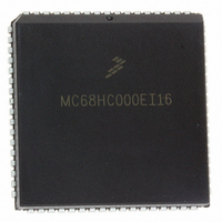
MC68HC000EI16 Freescale Semiconductor, MC68HC000EI16 Datasheet - Page 33

MC68HC000EI16
Manufacturer Part Number
MC68HC000EI16
Description
IC MPU 32BIT 16MHZ 68-PLCC
Manufacturer
Freescale Semiconductor
Specifications of MC68HC000EI16
Processor Type
M680x0 32-Bit
Speed
16MHz
Voltage
3.3V, 5V
Mounting Type
Surface Mount
Package / Case
68-PLCC
Family Name
M68000
Device Core
ColdFire
Device Core Size
16/32Bit
Frequency (max)
16MHz
Instruction Set Architecture
RISC
Supply Voltage 1 (typ)
5V
Operating Supply Voltage (max)
5.25V
Operating Supply Voltage (min)
4.75V
Operating Temp Range
0C to 70C
Operating Temperature Classification
Commercial
Mounting
Surface Mount
Pin Count
68
Package Type
PLCC
Lead Free Status / RoHS Status
Lead free / RoHS Compliant
Features
-
Lead Free Status / Rohs Status
Compliant
Available stocks
Company
Part Number
Manufacturer
Quantity
Price
Company:
Part Number:
MC68HC000EI16
Manufacturer:
TI
Quantity:
604
Company:
Part Number:
MC68HC000EI16
Manufacturer:
FREESCALE
Quantity:
2 900
Company:
Part Number:
MC68HC000EI16
Manufacturer:
Freescale Semiconductor
Quantity:
10 000
Company:
Part Number:
MC68HC000EI16R2
Manufacturer:
FREESCAL
Quantity:
8 831
Company:
Part Number:
MC68HC000EI16R2
Manufacturer:
Freescale Semiconductor
Quantity:
10 000
Data Strobe (
Data Transfer Acknowledge (
3.4 BUS ARBITRATION CONTROL
The bus request, bus grant, and bus grant acknowledge signals form a bus arbitration
circuit to determine which device becomes the bus master device. In the 48-pin version of
the MC68008 and MC68EC000, no pin is available for the bus grant acknowledge signal;
this microprocessor uses a two-wire bus arbitration scheme. All M68000 processors can
use two-wire bus arbitration.
MOTOROLA
This three-state signal and R/W control the flow of data on the data bus of the
MC68008. Table 3-2 lists the combinations of these signals and the corresponding data
on the bus. When the R/W line is high, the processor reads from the data bus. When
the R/W line is low, the processor drives the data bus.
This input signal indicates the completion of the data transfer. When the processor
recognizes DTACK during a read cycle, data is latched, and the bus cycle is terminated.
When DTACK is recognized during a write cycle, the bus cycle is terminated.
DS
*These conditions are a result of current implementation and may not appear
on future devices.
) (MC68008)
M68000 8-/16-/32-BIT MICROPROCESSORS USER'S MANUAL
High
High
High
UDS
Low
Low
Low
Low
Table 3-1. Data Strobe Control of Data Bus
DS
1
0
0
High
High
High
LDS
Low
Low
Low
Low
Table 3-2. Data Strobe Control
DTACK
R/
of Data Bus (MC68008)
—
1
0
W
High
High
High
R/
Low
Low
Low
—
W
).
Valid Data Bits 7–0 (Read Cycle)
Valid Data Bits 7–0 (Write Cycle)
Valid Data Bits
Valid Data Bus
Valid Data Bits
Valid Data Bits
Valid Data Bits
No Valid Data
No Valid Data
D8–D15
No Valid Data
15–8
15–8
15–8
7–0*
15–8
D0–D7
Valid Data Bits
Valid Data Bits
Valid Data Bits
Valid Data Bits
Valid Data Bits
No Valid Data
No Valid Data
D0–D7
15–8*
7–0
7–0
7–0
7–0
3- 5


