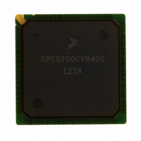
SPC5200CVR400B Freescale Semiconductor, SPC5200CVR400B Datasheet - Page 46

SPC5200CVR400B
Manufacturer Part Number
SPC5200CVR400B
Description
IC MPU 32BIT 400MHZ 272-PBGA
Manufacturer
Freescale Semiconductor
Datasheet
1.MPC5200VR400B.pdf
(72 pages)
Specifications of SPC5200CVR400B
Processor Type
MPC52xx PowerPC 32-Bit
Speed
400MHz
Voltage
1.5V
Mounting Type
Surface Mount
Package / Case
272-PBGA
Core Size
32 Bit
No. Of I/o's
56
Program Memory Size
32KB
Ram Memory Size
16KB
Cpu Speed
400MHz
Embedded Interface Type
CAN, I2C, SCI, SPI, USB
Digital Ic Case Style
BGA
Rohs Compliant
Yes
Family Name
MPC52xx
Device Core
PowerPC
Device Core Size
32b
Frequency (max)
400MHz
Instruction Set Architecture
RISC
Supply Voltage 1 (typ)
1.5V
Operating Supply Voltage (max)
1.58V
Operating Supply Voltage (min)
1.42V
Operating Temp Range
-40C to 85C
Operating Temperature Classification
Industrial
Mounting
Surface Mount
Pin Count
272
Package Type
BGA
Lead Free Status / RoHS Status
Lead free / RoHS Compliant
Features
-
Lead Free Status / Rohs Status
Compliant
Available stocks
Company
Part Number
Manufacturer
Quantity
Price
Company:
Part Number:
SPC5200CVR400B
Manufacturer:
SEMIKRON
Quantity:
200
Company:
Part Number:
SPC5200CVR400B
Manufacturer:
Freescale Semiconductor
Quantity:
10 000
Part Number:
SPC5200CVR400BL25R
Manufacturer:
FREESCALE
Quantity:
20 000
Company:
Part Number:
SPC5200CVR400BM62CREV1
Manufacturer:
FRRESCAL..
Quantity:
2 831
Company:
Part Number:
SPC5200CVR400BR2
Manufacturer:
Freescale Semiconductor
Quantity:
10 000
1.3.15
See the MPC5200B User’s Manual (MPC5200BUM).
46
1
2
3
Programming IFDR with the maximum frequency (IFDR=0x20) results in the minimum output timings listed. The
I
position is affected by the prescale and division values programmed in IFDR.
Because SCL and SDA are open-drain-type outputs, which the processor can only actively drive low, the time SCL
or SDA takes to reach a high level depends on external signal capacitance and pull-up resistor values.
Inter Peripheral Clock is defined in the MPC5200B User’s Manual (MPC5200BUM).
Sym
SCL
SDA
2
1
3
2
4
5
6
7
8
9
C interface is designed to scale the data transition time, moving it to the middle of the SCL low period. The actual
(2)
(1)
(1)
(1)
(1)
(1)
(1)
(1)
(1)
J1850
Start condition setup time (for repeated start condition
1
Table 41. I
Stop condition setup time
Start condition hold time
2
SCL/SDA rise time
SCL/SDA fall time
Figure 36. Timing Diagram—I
Data setup time
Clock high time
Clock low time
Data hold time
Output timing is specified at a nominal 50 pF load.
Description
2
C Output Timing Specifications—SCL and SDA
only)
4
MPC5200B Data Sheet, Rev. 4
6
NOTE
7
2
C Input/Output
Min
10
10
20
10
—
—
6
7
2
8
5
Max
7.9
7.9
—
—
—
—
—
—
—
3
IP-Bus Cycle
IP-Bus Cycle
IP-Bus Cycle
IP-Bus Cycle
IP-Bus Cycle
IP-Bus Cycle
IP-Bus Cycle
Units
Freescale Semiconductor
ns
ns
9
(3)
(3)
(3)
(3)
(3)
(3)
(3)
SpecID
A13.10
A13.11
A13.12
A13.13
A13.14
A13.15
A13.16
A13.8
A13.9


