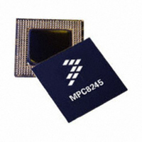
MPC8245LZU350D Freescale Semiconductor, MPC8245LZU350D Datasheet - Page 45

MPC8245LZU350D
Manufacturer Part Number
MPC8245LZU350D
Description
IC MPU 32BIT 350MHZ PPC 352-TBGA
Manufacturer
Freescale Semiconductor
Series
PowerPCr
Datasheet
1.MPC8245LZU266D.pdf
(68 pages)
Specifications of MPC8245LZU350D
Processor Type
MPC82xx PowerQUICC II 32-bit
Speed
350MHz
Voltage
2V
Mounting Type
Surface Mount
Package / Case
352-TBGA
Core Size
32 Bit
Program Memory Size
32KB
Cpu Speed
350MHz
Digital Ic Case Style
BGA
No. Of Pins
352
Supply Voltage Range
1.9V To 2.2V
Operating Temperature Range
0°C To +105°C
Rohs Compliant
No
Lead Free Status / RoHS Status
Contains lead / RoHS non-compliant
Features
-
Available stocks
Company
Part Number
Manufacturer
Quantity
Price
Company:
Part Number:
MPC8245LZU350D
Manufacturer:
MOTOROLA
Quantity:
586
Company:
Part Number:
MPC8245LZU350D
Manufacturer:
Freescale Semiconductor
Quantity:
10 000
Part Number:
MPC8245LZU350D
Manufacturer:
FREESCALE
Quantity:
20 000
7.3
To ensure reliable operation, connect unused inputs to an appropriate signal level. Tie unused active-low
inputs to OV
Power and ground connections must be made to all external V
The PCI_SYNC_OUT signal is to be routed halfway out to the PCI devices and returned to the
PCI_SYNC_IN input of the MPC8245.
The SDRAM_SYNC_OUT signal is to be routed halfway out to the SDRAM devices and then returned to
the SDRAM_SYNC_IN input of the MPC8245. The trace length can be used to skew or adjust the timing
window as needed. See the Tundra Tsi107™ Design Guide (AN1849) and Freescale application notes
AN2164, MPC8245/MPC8241 Memory Clock Design Guidelines: Part 1 and AN2746,
MPC8245/MPC8241 Memory Clock Design Guidelines: Part 2 for details. Note that there is an
SDRAM_SYNC_IN to PCI_SYNC_IN time requirement (refer to
specifications).
7.4
The data bus input receivers are normally turned off when no read operation is in progress; therefore, they
do not require pull-up resistors on the bus. The data bus signals are: MDH[0:31], MDL[0:31], and
PAR[0:7].
If the 32-bit data bus mode is selected, the input receivers of the unused data and parity bits (MDL[0:31]
and PAR[4:7]) are disabled, and their outputs drive logic zeros when they would otherwise normally be
driven. For this mode, these pins do not require pull-up resistors and should be left unconnected to
minimize possible output switching.
The TEST0 pin requires a pull-up resistor of 120 Ω or less connected to OV
RTC should have weak pull-up resistors (2–10 kΩ) connected to GV
The following signals should be pulled up to OV
SMI, SRESET/SDMA12, TBEN/SDMA13, CHKSTOP_IN/SDMA14, TRIG_IN/RCS2, INTA,
QACK/DA0 and DRDY. Note that QACK/DA0 should be left without a pull-up resistor only if an external
clock is used because this signal enables internal clock flipping logic when it is low on reset, which is
necessary when the PLL[0:4] signals select a half-clock frequency ratio and an external PLL is used to
drive the SDRAM device.
It is recommended that the following PCI control signals be pulled up to LV
weak pull-up resistors (2–10 kΩ): DEVSEL, FRAME, IRDY, LOCK, PERR, SERR, STOP, and TRDY.
The resistor values may need to be adjusted stronger to reduce induced noise on specific board designs.
The following pins have internal pull-up resistors enabled at all times: REQ[3:0], REQ4/DA4, TCK, TDI,
TMS, and TRST. See
The following pins have internal pull-up resistors enabled only while device is in the reset state:
GNT4/DA5, MDL0, FOE, RCS0, SDRAS, SDCAS, CKE, AS, MCP, MAA[0:2], and PMAA[0:2]. See
Table
Freescale Semiconductor
16.
Connection Recommendations
Pull-Up/Pull-Down Resistor Requirements
DD
. Connect unused active-high inputs tie to GND. All NC signals must remain unconnected.
Table
MPC8245 Integrated Processor Hardware Specifications, Rev. 10
16.
DD
with weak pull-up resistors (2–10 kΩ): SDA, SCL,
DD
, OV
Table 10
DD
DD
.
, GV
DD
for the input AC timing
DD
(the clamping voltage) with
DD
.
, LV
DD
, and GND pins.
System Design
45


