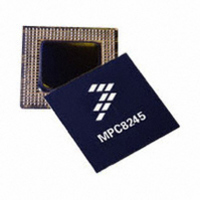
MPC8245LVV266D Freescale Semiconductor, MPC8245LVV266D Datasheet - Page 3

MPC8245LVV266D
Manufacturer Part Number
MPC8245LVV266D
Description
IC MPU 32BIT 266MHZ PPC 352-TBGA
Manufacturer
Freescale Semiconductor
Series
PowerQUICC IIr
Datasheet
1.MPC8245LZU266D.pdf
(68 pages)
Specifications of MPC8245LVV266D
Processor Type
MPC82xx PowerQUICC II 32-bit
Speed
266MHz
Voltage
1.8V
Mounting Type
Surface Mount
Package / Case
352-TBGA
Core Size
32 Bit
Program Memory Size
32KB
Cpu Speed
266MHz
Embedded Interface Type
I2C, UART
Digital Ic Case Style
TBGA
No. Of Pins
352
Supply Voltage Range
1.7V To 2.1V
Rohs Compliant
Yes
Lead Free Status / RoHS Status
Lead free / RoHS Compliant
Features
-
Available stocks
Company
Part Number
Manufacturer
Quantity
Price
Company:
Part Number:
MPC8245LVV266D
Manufacturer:
Freescal
Quantity:
672
Company:
Part Number:
MPC8245LVV266D
Manufacturer:
Freescale Semiconductor
Quantity:
10 000
Part Number:
MPC8245LVV266D
Manufacturer:
FREESCALE
Quantity:
20 000
The peripheral logic integrates a PCI bridge, dual universal asynchronous receiver/transmitter (DUART),
memory controller, DMA controller, PIC interrupt controller, a message unit (and I
I
support, memory management, a 16-Kbyte instruction cache, a 16-Kbyte data cache, and power
management features. The integration reduces the overall packaging requirements and the number of
discrete devices required for an embedded system.
An internal peripheral logic bus interfaces the processor core to the peripheral logic. The core can operate
at a variety of frequencies, allowing the designer to trade off performance for power consumption. The
processor core is clocked from a separate PLL that is referenced to the peripheral logic PLL. This allows
the microprocessor and the peripheral logic block to operate at different frequencies while maintaining a
synchronous bus interface. The interface uses a 64- or 32-bit data bus (depending on memory data bus
width) and a 32-bit address bus along with control signals that enable the interface between the processor
and peripheral logic to be optimized for performance. PCI accesses to the MPC8245 memory space are
passed to the processor bus for snooping when snoop mode is enabled.
The general-purpose processor core and peripheral logic serve a variety of embedded applications. The
MPC8245 can be used as either a PCI host or PCI agent controller.
2
Major features of the MPC8245 are as follows:
Freescale Semiconductor
2
C controller. The processor core is a full-featured, high-performance processor with floating-point
•
•
Features
Processor core
— High-performance, superscalar processor core
— Integer unit (IU), floating-point unit (FPU) (software enabled or disabled), load/store unit
— 16-Kbyte instruction cache
— 16-Kbyte data cache
— Lockable L1 caches—Entire cache or on a per-way basis up to three of four ways
— Dynamic power management: 60x nap, doze, and sleep modes
Peripheral logic
— Peripheral logic bus
— Memory interface
(LSU), system register unit (SRU), and branch processing unit (BPU)
– Various operating frequencies and bus divider ratios
– 32-bit address bus, 64-bit data bus
– Full memory coherency
– Decoupled address and data buses for pipelining of peripheral logic bus accesses
– Store gathering on peripheral logic bus-to-PCI writes
– Up to 2 Gbytes of SDRAM memory
– High-bandwidth data bus (32- or 64-bit) to SDRAM
– Programmable timing supporting SDRAM
– One to eight banks of 16-, 64-, 128-, 256-, or 512-Mbit memory devices
MPC8245 Integrated Processor Hardware Specifications, Rev. 10
2
O interface), and an
Features
3


