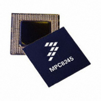
MPC8245ARZU400D Freescale Semiconductor, MPC8245ARZU400D Datasheet - Page 11

MPC8245ARZU400D
Manufacturer Part Number
MPC8245ARZU400D
Description
IC MPU 32BIT 400MHZ 352-TBGA
Manufacturer
Freescale Semiconductor
Datasheet
1.MPC8245ARZU400D.pdf
(16 pages)
Specifications of MPC8245ARZU400D
Processor Type
MPC82xx PowerQUICC II 32-bit
Speed
400MHz
Voltage
2.1V
Mounting Type
Surface Mount
Package / Case
352-TBGA
Processor Series
MPC8xxx
Core
603e
Data Bus Width
32 bit
Maximum Clock Frequency
400 MHz
Operating Supply Voltage
2 V, 2.1 V, 3.3 V
Maximum Operating Temperature
+ 105 C
Mounting Style
SMD/SMT
Minimum Operating Temperature
0 C
Lead Free Status / RoHS Status
Contains lead / RoHS non-compliant
Features
-
Lead Free Status / Rohs Status
Lead free / RoHS Compliant
Available stocks
Company
Part Number
Manufacturer
Quantity
Price
Company:
Part Number:
MPC8245ARZU400D
Manufacturer:
Freescale Semiconductor
Quantity:
10 000
Part Number:
MPC8245ARZU400D
Manufacturer:
FREESCALE
Quantity:
20 000
Freescale Semiconductor
Notes:
1.
2.
3.
4.
5.
6.
7.
8.
9.
10. In clock off mode, no clocking occurs inside the MPC8245, regardless of the PCI_SYNC_IN input.
11. Range values are shown rounded down to the nearest whole number (decimal place accuracy removed) for
12. PLL_CFG[0:4] settings that are not listed are reserved.
13. Multiplier ratios for this PLL_CFG[0:4] setting are different from the MPC8240 and are not
14. PCI_SYNC_IN range for this PLL_CFG[0:4] setting is different from the MPC8240 and may not be fully
15. Bits 7–4 of register offset <0xE2> contain the PLL_CFG[0:4] setting value.
16. In PLL bypass mode, the PCI_SYNC_IN input signal clocks the internal processor directly, the peripheral
17. In dual PLL bypass mode, the PCI_SYNC_IN input signal clocks the internal peripheral logic directly, the
1E (Rev. B)
1E (Rev. D)
Limited by maximum PCI input frequency (66 MHz).
Limited by maximum system memory interface operating frequency (133 MHz).
Limited by minimum memory VCO frequency (132 MHz).
Limited due to maximum memory VCO frequency (372 MHz).
Limited by maximum CPU operating frequency (400 MHz).
Limited by minimum CPU VCO frequency (360 MHz).
Limited by maximum CPU VCO frequency (800 MHz).
Limited by minimum CPU operating frequency (100 MHz).
Limited by minimum memory bus frequency (50 MHz).
clarity.
backwards-compatible.
backwards-compatible.
logic PLL is disabled, and the bus mode is set for 1:1 (PCI:Mem) mode operation. This mode is intended for
hardware modeling support. The AC timing specifications given in this document do not apply in the PLL
bypass mode.
peripheral logic PLL is disabled, and the bus mode is set for 1:1 (PCI_SYNC_IN:Mem) mode operation. In
this mode, the OSC_IN input signal clocks the internal processor directly in 1:1 (OSC_IN:CPU) mode
operation, and the processor PLL is disabled. The PCI_SYNC_IN and OSC_IN input clocks must be
externally synchronized. This mode is intended for hardware modeling support. The AC timing specifications
given in this document do not apply in the dual PLL bypass mode.
Ref
1A
1B
1C
1D
17
18
19
1F
MPC8245 Hardware Specifications Addendum for the MPC8245ARXXnnnx Series, Rev. 3
Table 18. PLL Configurations for the 400-MHz Part Offering (continued)
[0:4]
PLL_CFG
11011
11110
11111
10111
11000
11001
11010
11100
11101
11110
11,14,15
13
10
10
PCI Clock Input
(PCI_SYNC_IN)
Range
27
36
50
34
44
48
33
25–33
(MHz)
3
6
9
3
6
6
3
–53
–66
–66
–66
–66
–66
–57
2
1
5
1
1
1
1
1
5
400-MHz Part
Not usable
Not usable
Logic/Mem
Bus Clock
100–132
68–132
72–132
68–132
66–114
Periph
Range
(MHz)
50–66
66–99
72–99
9
CPU Clock
200–264
204–396
180–330
200–264
204–396
198–297
180–248
231–399
Range
(MHz)
PCI-to-Mem
(Mem VCO)
2.5 (2)
1.5 (2)
1.5 (2)
4 (2)
2 (2)
1 (4)
2 (2)
2 (2)
Off
Off
Multipliers
Mem-to-CPU
(CPU VCO)
2.5 (2)
2.5 (2)
3.5 (2)
2 (2)
3 (2)
4 (2)
3 (2)
3 (2)
PLL Configuration
Off
Off
11


