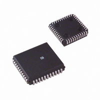
AD1849KP-REEL Analog Devices Inc, AD1849KP-REEL Datasheet - Page 12

AD1849KP-REEL
Manufacturer Part Number
AD1849KP-REEL
Description
IC CODEC STEREO 5V 16BIT 44PLCC
Manufacturer
Analog Devices Inc
Type
Stereo Audior
Datasheet
1.AD1849KP.pdf
(28 pages)
Specifications of AD1849KP-REEL
Rohs Status
RoHS non-compliant
Data Interface
Serial
Resolution (bits)
16 b
Number Of Adcs / Dacs
2 / 2
Sigma Delta
Yes
Dynamic Range, Adcs / Dacs (db) Typ
83 / 86
Voltage - Supply, Analog
4.75 V ~ 5.25 V
Voltage - Supply, Digital
4.75 V ~ 5.25 V
Operating Temperature
0°C ~ 70°C
Mounting Type
Surface Mount
Package / Case
44-PLCC
AD1849K
Control Byte 2, Data Format Register
DFR2:0
ST
DF1:0
Control Byte 3, Serial Port Control Register
ITS
MCK2:0
FSEL1:0
MS
TXDIS
Data 7
Data 7
ITS
Data conversion frequency (F
DFR
Note that the AD1849K’s internal oscillators can be overdriven by external clock sources at the crystal input pins. If an
external clock source is used, it should be applied to the crystal input pin (CIN1 or CIN2), and the crystal output pin
(COUT1 or COUT2) should be left unconnected. The external clock source need not be at the recommended crystal
frequencies, and it will be divided down by the selected Divide Factor.
Global stereo mode. Both converters are placed in the same mode.
Codec data format selection:
Immediate three-state:
Clock source select for Codec internal operation:
Frame size select:
Note that FSEL is overridden in Data Mode when SCLK is the clock source (MCK = “0”). When SCLK is providing
the 256 × F
Master/slave mode for the serial interface:
Transmitter disable:
Note that Control Mode overrides TXDIS. In Control Mode, the serial output is always enabled.
55
47
Note that MS is overridden when SCLK is the clock source (MCK = “0”). When SCLK is providing the clock for
internal Codec operation, slave mode is effectively selected, regardless of the contents of MS.
0
0
1
2
3
4
5
6
7
0
1
0
1
2
3
0
1
0
1
2
3
4
0
1
2
3
0
1
0
1
Mono mode. The left analog input appears at both ADC outputs. The left digital input appears at both DAC outputs.
Stereo mode
16-bit twos-complement PCM linear
8-bit µ-law companded
8-bit A-law companded
8-bit unsigned PCM linear
FSYNC, SDTX and SCLK three-state within 3 SCLK cycles after D/C goes LO
FSYNC, SDTX and SCLK three-state immediately after D/C goes LO
Serial bit clock (SCLK) is the master clock at 256 × F
24.576 MHz crystal (XTAL1) is the clock source
16.9344 MHz crystal (XTAL2) is the clock source
External clock (CLKIN) is the clock source at 256 × F
External clock (CLKIN) is the clock source, divided by the factor selected by DFR2:0
(External clock must be stable and valid within 2000 periods after it is selected.)
64 bits per frame
128 bits per frame
256 bits per frame
Reserved
Receive serial clock (SCLK) and TSIN from an external device (“slave mode”)
Transmit serial clock (SCLK) and frame sync (FSYNC) to external devices (“master mode”)
Enable serial output
Three-state serial data output (high impedance)
Divide Factor
3072
1536
896
768
448
384
512
2560
S
clock for internal Codec operation, 256 bits per frame is effectively selected, regardless of FSEL’s contents.
Data 6
Data 6
MCK2
54
46
0
Data 5
Data 5
MCK1
DFR2
S
) select tin kHz:
53
45
Data 4
Data 4
MCK0
DFR1
52
44
XTAL1 (24.576 MHz)
8
16
27.42857
32
N/A
N/A
48
9.6
Data 3
Data 3
FSEL1
DFR0
S
S
51
43
Data 2
Data 2
FSEL0
ST
50
42
XTAL2 (16.9344 MHz)
5.5125
11.025
18.9
22.05
37.8
44.1
33.075
6.615
Data 1
Data 1
DF1
MS
49
41
TXDIS
Data 0
Data 0
DF0
48
40


