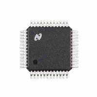
LM4549VH National Semiconductor, LM4549VH Datasheet - Page 9

LM4549VH
Manufacturer Part Number
LM4549VH
Description
IC CODEC AC '97 REV 2.1 48LQFP
Manufacturer
National Semiconductor
Type
Audio Codec '97r
Specifications of LM4549VH
Data Interface
Serial
Resolution (bits)
18 b
Number Of Adcs / Dacs
2 / 2
Sigma Delta
Yes
Dynamic Range, Adcs / Dacs (db) Typ
90 / 89
Voltage - Supply, Analog
4.2 V ~ 5.5 V
Voltage - Supply, Digital
3 V ~ 5.5 V
Operating Temperature
-40°C ~ 85°C
Mounting Type
Surface Mount
Package / Case
48-LQFP
Single Supply Voltage (typ)
3.3/5V
Single Supply Voltage (min)
3/4.2V
Single Supply Voltage (max)
5.5V
Package Type
LQFP
Lead Free Status / RoHS Status
Contains lead / RoHS non-compliant
Other names
*LM4549VH
Available stocks
Company
Part Number
Manufacturer
Quantity
Price
Company:
Part Number:
LM4549VH
Manufacturer:
NATIONAL
Quantity:
27
Part Number:
LM4549VHX
Manufacturer:
NS/国半
Quantity:
20 000
SDATA_OUT
SDATA_IN
VREFOUT
XTL_OUT
3DP, 3DN
Pin Description
Digital I/O and Clocking
Power Supplies and References
BIT_CLK
RESET#
XTL_IN
AFILT1
AFILT2
Name
SYNC
EAPD
Name
AVDD
DVDD
DVSS
AVSS
VREF
ID0
ID1
33,34
Pin
Pin
1,9
4,7
10
11
45
46
47
25
26
27
28
29
30
2
3
5
6
8
I / O
I / O
I/O
(Continued)
O
O
O
O
O
O
O
O
I
I
I
I
I
I
I
I
I
I
24.576 MHz crystal input. Use a fundamental-mode type crystal. When operating from a
crystal, a 1M
24.576 MHz crystal output. When operating from a crystal, a 1M
connected across pins 2 and 3.
This data stream contains both control data and DAC audio data. This input is sampled by
the LM4549 on the falling edge of BIT_CLK.
OUTPUT when in Primary Codec Mode: This pin outputs a 12.288 MHz clock which is
derived (internally divided by two) from the 24.576MHz crystal input (XTL_IN).
INPUT when in Secondary Codec Mode (Multiple Codec configurations only): 12.288MHz
clock is to be supplied from an external source, such as from the BIT_CLK of a Primary
Codec.
This data stream contains both control data and ADC audio data. This output is clocked out
by the LM4549 on the rising edge of BIT_CLK.
48kHz sync pulse which signifies the beginning of both the SDATA_IN and SDATA_OUT
serial streams. SYNC must be synchronous to BIT_CLK.
This active low signal causes a hardware reset which returns the control registers to their
default conditions.
ID0 and ID1 set the codec address for multiple codec use where ID0 is the LSB. Connect
these pins to DVdd or GND as required. If these pins are not connected (NC), they default
to Primary codec setting (same as connecting both pins to DVdd). These pins are of inverted
polarity relative to their internal ID0, ID1 registers. If pin 45 is connected to GND, then ID0
will be set to 1 internally. Connection to DVdd corresponds to a 0 internally.
ID0 and ID1 set the codec address for multiple codec use where ID1 is the MSB. Connect
these pins to DVdd or GND as required. If these pins are not connected (NC), they default
to Primary codec setting (same as connecting both pins to DVdd). These pins are of inverted
polarity relative to their internal ID0, ID1 registers. If pin46 is connected to GND, then ID1
will be set to 1 internally. Connection to DVdd corresponds to a 0 internally.
The contents of Powerdown Ctrl/Stat register 26h bit 15 determines the logic level output
on this pin. This pin is to be connected to an external power amplifier’s shutdown pin. If
EAPD=0, then a logic low is output and the external amplifer is enabled. If EAPD=1, the
amplifer is shutdown. Power up default is EAPD=0.
Analog supply.
Analog ground.
Digital supply.
Digital ground.
Nominal 2.2V reference output. Not intended to sink or source current. Bypassing of this pin
should be done with short traces to maximize performance.
Nominal 2.2V reference output. Can source up to 5mA of current and can be used to bias a
microphone.
This pin is not used and should be left open (NC). However, a capacitor to ground on this
pin is permitted - it will not affect performance.
This pin is not used and should be left open (NC). However, a capacitor to ground on this
pin is permitted - it will not affect performance.
These pins are used to complete the National 3D Sound circuit. Connect a 0.022µF
capacitor between pins 3DP and 3DN. The National 3D Sound can be turned on and off via
bit D13 in control register 20h. This is a fixed-depth type stereo enhance circuit, thus writing
to register 22h has no effect. If National 3D Sound is not needed, then these pins should be
left as no connect (NC).
resistor must be connected across pins 2 and 3.
9
Functional Description
Functional Description
resistor must be
www.national.com


