LTC4263IDE-1#TRPBF Linear Technology, LTC4263IDE-1#TRPBF Datasheet - Page 8
LTC4263IDE-1#TRPBF
Manufacturer Part Number
LTC4263IDE-1#TRPBF
Description
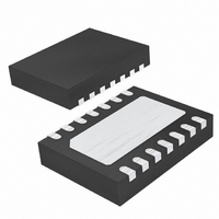
IC IEEE 803.2AF CNTRLR 14-DFN
Manufacturer
Linear Technology
Type
Power Over Ethernet (PoE)r
Datasheet
1.LTC4263CDE-1PBF.pdf
(20 pages)
Specifications of LTC4263IDE-1#TRPBF
Applications
Power Interface Switch for Power Over Ethernet (PoE) Devices
Voltage - Supply
48V
Operating Temperature
-40°C ~ 85°C
Mounting Type
Surface Mount
Package / Case
14-DFN
Current - Supply
1mA
Interface
IEEE 802.3af
Controller Type
Power Sourcing Equipment Controller (PSE)
Lead Free Status / RoHS Status
Lead free / RoHS Compliant
Available stocks
Company
Part Number
Manufacturer
Quantity
Price


PIN FUNCTIONS
LTC4263-1
LED (Pin 1): Port State LED Drive. This pin is an open-
drain output that pulls down when the port is powered.
Under port fault conditions, the LED will fl ash in patterns
to indicate the nature of the port fault. See the Applications
Information section for a description of these patterns.
When the LTC4263-1 is operated from a single 48V sup-
ply, this pin is pulsed low with a 6% duty cycle during
the periods when the LED should be on. This allows use
of a simple inductor, diode, and resistor circuit to avoid
excess heating due to the large voltage drop from V
See the Applications Information section for details on
this circuit.
LEGACY (Pin 2): Legacy Detect. This pin controls whether
legacy detect is enabled. If held at V
enabled and testing for a large capacitor is performed to
detect the presence of a legacy PD on the port. See the
Applications Information section for descriptions of legacy
PDs that can be detected. If held at V
compliant PDs are detected. If left fl oating, the LTC4263-1
enters force-power-on mode and any PD that generates
between 1V and 10V when biased with 270μA of detection
current will be powered as a legacy device. This mode is
useful if the system uses a differential detection scheme
to detect legacy devices.
MIDSPAN (Pin 3): Midspan Enable. If this pin is connected
to V
delay occurs after every failed detect cycle unless the
result is open circuit. If held at V
failed detect cycles.
V
6 and 13 should be tied together on the PCB. For optimum
power delivery, supply voltage should be maximized. See
Applications Information section for more information.
OSC (Pin 7) Oscillator for AC Disconnect. If AC discon-
nect is used, connect a 0.1μF X7R capacitor from OSC to
V
DC disconnect.
8
SS
SS
. Tie OSC to V
DD5
(Pins 4, 5, 6, 13): Negative Power Supply. Pins 4, 5,
, Midspan backoff is enabled and a 3.2 second
SS
to disable AC disconnect and enable
SS
, no delay occurs after
SS
DD5
, only IEEE 802.3af
, legacy detect is
DD48
.
ACOUT (Pin 8): AC Disconnect Sense. Senses the port
to determine whether a PD is still connected when in AC
disconnect mode. If port capacitance drops below about
0.15μF for longer than T
AC disconnect is used, connect this pin to the port with
a series combination of a 1k resistor and a 0.47μF 100V
X7R capacitor. See the Applications Information section
for more information.
OUT (Pins 9, 10): Port Output. If DC disconnect is used,
these pins are connected to the port. If AC disconnect is
used, these pins are connected to the port through a parallel
combination of a 1A diode and a 500k resistor. Pins 9 and
10 should be tied together on the PCB. See the Applications
Information section for more information.
V
with a 0.1μF capacitor to V
supply voltage should be maximized. See Applications
Information section for more information.
SD (Pin 12): Shutdown. If held low, the LTC4263-1 is
prevented from performing detection or powering the port.
Pulling SD low will turn off the port if it is powered. When
released, a 4-second delay will occur before detection is
attempted. If not used, tie to V
V
to V
bypass capacitor to V
When the internal regulator is used, this pin should only
be connected to the bypass capacitor and to any logic pins
of the LTC4263-1 that are being held at V
Exposed Pad (Pin 15): V
on the PCB. The Exposed Pad acts as a heat sink for the
internal MOSFET.
DD48
DD5
SS
(Pin 14): Logic Power Supply. Apply 5V referenced
(Pin 11): Power Return for V
, if such a supply is available, or place a 0.1μF
SS
to enable the internal regulator.
SS
MPDO
SS
. For optimum power delivery,
. Must be connected to V
DD5
the port is turned off. If
.
SS
. Must be bypassed
DD5
.
42631fa
SS
Related parts for LTC4263IDE-1#TRPBF
Image
Part Number
Description
Manufacturer
Datasheet
Request
R

Part Number:
Description:
IC IEEE 803.2AF CNTRLR 14-DFN
Manufacturer:
Linear Technology
Datasheet:
Part Number:
Description:
IC IEEE 803.2AF CNTRLR 14-DFN
Manufacturer:
Linear Technology
Datasheet:
Part Number:
Description:
IC IEEE 803.2AF CNTRLR 14DFN
Manufacturer:
Linear Technology
Datasheet:

Part Number:
Description:
IC,Power Control/Management,CMOS,LLCC,14PIN,PLASTIC
Manufacturer:
Linear Technology
Part Number:
Description:
IC,Power Control/Management,CMOS,LLCC,14PIN,PLASTIC
Manufacturer:
Linear Technology
Part Number:
Description:
CD ROM LINEARVIEW DATASHEETS
Manufacturer:
Linear Technology

Part Number:
Description:
Standalone Linear Li-Ion Battery Charger with Thermal Regulation in ThinSOT
Manufacturer:
Linear Technology Corporation
Datasheet:
Part Number:
Description:
Low noise, high frequency, 8th order linear phase lowpass filter
Manufacturer:
Linear Technology Corporation
Datasheet:
Part Number:
Description:
Manufacturer:
Linear Technology Corporation
Datasheet:
Part Number:
Description:
Manufacturer:
Linear Technology Corporation
Datasheet:
Part Number:
Description:
Manufacturer:
Linear Technology Corporation
Datasheet:
Part Number:
Description:
Manufacturer:
Linear Technology Corporation
Datasheet:
Part Number:
Description:
Manufacturer:
Linear Technology Corporation
Datasheet:
Part Number:
Description:
Manufacturer:
Linear Technology Corporation
Datasheet:
Part Number:
Description:
Manufacturer:
Linear Technology Corporation
Datasheet: