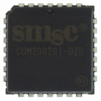
COM20020I-DZD SMSC, COM20020I-DZD Datasheet - Page 40

COM20020I-DZD
Manufacturer Part Number
COM20020I-DZD
Description
IC CTRLR LAN UNIV 2KX8 28-PLCC
Manufacturer
SMSC
Series
ARCNETr
Datasheet
1.COM20020I3V-DZD.pdf
(72 pages)
Specifications of COM20020I-DZD
Controller Type
ARCNET Controller
Interface
Differential
Voltage - Supply
4.5 V ~ 5.5 V
Current - Supply
20mA
Operating Temperature
-40°C ~ 85°C
Mounting Type
Surface Mount
Package / Case
28-PLCC
Product
Controller Area Network (CAN)
Number Of Transceivers
1
Data Rate
5 Mbps
Supply Voltage (max)
5.5 V
Supply Voltage (min)
4.5 V
Supply Current (max)
40 mA (Typ)
Maximum Operating Temperature
+ 85 C
Minimum Operating Temperature
- 40 C
Mounting Style
SMD/SMT
Lead Free Status / RoHS Status
Lead free / RoHS Compliant
Other names
638-1001-5
Available stocks
Company
Part Number
Manufacturer
Quantity
Price
Company:
Part Number:
COM20020I-DZD
Manufacturer:
Standard
Quantity:
17 665
Company:
Part Number:
COM20020I-DZD
Manufacturer:
SMSC
Quantity:
269
Company:
Part Number:
COM20020I-DZD
Manufacturer:
Microchip Technology
Quantity:
10 000
Company:
Part Number:
COM20020I-DZD-TR
Manufacturer:
Microchip Technology
Quantity:
10 000
6.3
6.3.1
6.3.2
6.4
Revision 12-05-06
Internal RAM
The integration of the 2K x 8 RAM in the COM20020ID represents significant real estate savings. The
most obvious benefit is the 48 pin package in which the device is now placed (a direct result of the
integration of RAM). In addition, the PC board is now free of the cumbersome external RAM, external
latch, and multiplexed address/data bus and control functions which were necessary to interface to the
RAM. The integration of RAM represents significant cost savings because it isolates the system designer
from the changing costs of external RAM and it minimizes reliability problems, assembly time and costs,
and layout complexity.
Sequential Access Memory
The internal RAM is accessed via a pointer-based scheme. Rather than interfering with system memory,
the internal RAM is indirectly accessed through the Address High and Low Pointer Registers. The data is
channeled to and from the microcontroller via the 8-bit data register. For example: a packet in the internal
RAM buffer is read by the microcontroller by writing the corresponding address into the Address Pointer
High and Low Registers (offsets 02H and 03H). Note that the High Register should be written first,
followed by the Low Register, because writing to the Low Register loads the address. At this point the
device accesses that location and places the corresponding data into the data register.
microcontroller then reads the data register (offset 04H) to obtain the data at the specified location. If the
Auto Increment bit is set to logic "1", the device will automatically increment the address and place the
next byte of data into the data register, again to be read by the microcontroller. This process is continued
until the entire packet is read out of RAM. Refer to Figure 6.1 for an illustration of the Sequential Access
operation. When switching between reads and writes, the pointer must first be written with the starting
address. At least one cycle time should separate the pointer being loaded and the first read (see timing
parameters).
Access Speed
The COM20020ID is able to accommodate very fast access cycles to its registers and buffers. Arbitration
to the buffer does not slow down the cycle because the pointer based access method allows data to be
prefetched from memory and stored in a temporary register. Likewise, data to be written is stored in the
temporary register and then written to memory.
For systems which do not require quick access time, the arbitration clock may be slowed down by setting
bit 0 of the Setup1 Register equal to logic "1". Since the Slow Arbitration feature divides the input clock by
two, the duty cycle of the input clock may be relaxed.
Software Interface
The microcontroller interfaces to the COM20020ID via software by accessing the various registers. These
actions are described in the Internal Registers section. The software flow for accessing the data buffer is
based on the Sequential Access scheme. The basic sequence is as follows:
Disable Interrupts
Write to Pointer Register High (specifying Auto-Increment mode)
Write to Pointer Register Low (this loads the address)
Enable Interrupts
Read or Write the Data Register (repeat as many times as necessary to empty or fill the buffer)
The pointer may now be read to determine how many transfers were completed.
DATASHEET
Page 40
5Mbps ARCNET (ANSI 878.1) Controller with 2K x 8 On-Chip RAM
SMSC COM20020I Rev D
Datasheet
The


