SJA1000T/N,112 NXP Semiconductors, SJA1000T/N,112 Datasheet - Page 5
SJA1000T/N,112
Manufacturer Part Number
SJA1000T/N,112
Description
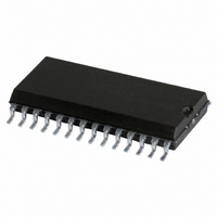
IC STAND-ALONE CAN CTRLR 28-SOIC
Manufacturer
NXP Semiconductors
Datasheet
1.SJA1000TN1112.pdf
(68 pages)
Specifications of SJA1000T/N,112
Controller Type
CAN Interface
Interface
CAN
Voltage - Supply
4.5 V ~ 5.5 V
Current - Supply
15mA
Operating Temperature
-40°C ~ 125°C
Mounting Type
Surface Mount
Package / Case
28-SOIC (7.5mm Width)
Lead Free Status / RoHS Status
Lead free / RoHS Compliant
Other names
935277294112
SJA1000T/N
SJA1000T/N
SJA1000T/N
SJA1000T/N


Philips Semiconductors
5
Note
1. XTAL1 and XTAL2 pins should be connected to V
2000 Jan 04
AD7 to AD0
ALE/AS
CS
RD/E
WR
CLKOUT
V
XTAL1
XTAL2
MODE
V
TX0
TX1
V
INT
RST
V
RX0, RX1
V
V
SS1
DD3
SS3
DD2
SS2
DD1
Stand-alone CAN controller
SYMBOL
PINNING
2, 1, 28 to 23
19, 20
PIN
10
11
12
13
14
15
16
17
18
21
22
3
4
5
6
7
8
9
chip select input, LOW level allows access to the SJA1000
RD signal (Intel mode) or E enable signal (Motorola mode) from the microcontroller
WR signal (Intel mode) or RD/WR signal (Motorola mode) from the microcontroller
clock output signal produced by the SJA1000 for the microcontroller; the clock
signal is derived from the built-in oscillator via the programmable divider; the clock
off bit within the clock divider register allows this pin to disable
5 V supply for output driver
output from the CAN output driver 0 to the physical bus line
output from the CAN output driver 1 to the physical bus line
ground for output driver
interrupt output, used to interrupt the microcontroller; INT is active LOW if any bit of
be a wired-OR with other INT outputs within the system; a LOW level on this pin will
reactivate the IC from sleep mode
reset input, used to reset the CAN interface (active LOW); automatic power-on reset
can be obtained by connecting RST via a capacitor to V
(e.g. C = 1 F; R = 50 k )
5 V supply for input comparator
a dominant level will wake up the SJA1000 if sleeping; a dominant level is read, if
RX1 is higher than RX0 and vice versa for the recessive level; if the CBP bit (see
Table 49) is set in the clock divider register, the CAN input comparator is bypassed
to achieve lower internal delays if an external transceiver circuitry is connected to
the SJA1000; in this case only RX0 is active; HIGH is interpreted as recessive level
and LOW is interpreted as dominant level
ground for input comparator
5 V supply for logic circuits
multiplexed address/data bus
ALE input signal (Intel mode), AS input signal (Motorola mode)
ground for logic circuits
input to the oscillator amplifier; external oscillator signal is input via this pin; note 1
output from the oscillator amplifier; the output must be left open-circuit when an
external oscillator signal is used; note 1
mode select input
the internal interrupt register is set; INT is an open-drain output and is designed to
input from the physical CAN-bus line to the input comparator of the SJA1000;
1 = selects Intel mode
0 = selects Motorola mode
SS1
via 15 pF capacitors.
5
DESCRIPTION
SS
and a resistor to V
Product specification
SJA1000
DD
Related parts for SJA1000T/N,112
Image
Part Number
Description
Manufacturer
Datasheet
Request
R

Part Number:
Description:
IC STAND-ALONE CAN CTRLR 28-SOIC
Manufacturer:
NXP Semiconductors
Datasheet:
Part Number:
Description:
IC STAND-ALONE CAN CTRLR 28-SOIC
Manufacturer:
NXP Semiconductors
Datasheet:

Part Number:
Description:
Manufacturer:
NXP Semiconductors
Datasheet:
Part Number:
Description:
IC STAND-ALONE CAN CTRLR 28-SOIC
Manufacturer:
NXP Semiconductors
Datasheet:
Part Number:
Description:
Manufacturer:
NXP Semiconductors
Datasheet:
Part Number:
Description:
Manufacturer:
NXP Semiconductors
Datasheet:
Part Number:
Description:
Manufacturer:
NXP Semiconductors
Datasheet:

Part Number:
Description:
CONTROLLER, CAN, STANDALONE, 28SOIC
Manufacturer:
NXP Semiconductors
Datasheet:
Part Number:
Description:
Stand-alone Can Controller
Manufacturer:
NXP Semiconductors
Datasheet:
Part Number:
Description:
Network Controller & Processor ICs STAND ALONE CAN CONTROLLER
Manufacturer:
NXP Semiconductors
Datasheet:
Part Number:
Description:
NXP Semiconductors designed the LPC2420/2460 microcontroller around a 16-bit/32-bitARM7TDMI-S CPU core with real-time debug interfaces that include both JTAG andembedded trace
Manufacturer:
NXP Semiconductors
Datasheet:

Part Number:
Description:
NXP Semiconductors designed the LPC2458 microcontroller around a 16-bit/32-bitARM7TDMI-S CPU core with real-time debug interfaces that include both JTAG andembedded trace
Manufacturer:
NXP Semiconductors
Datasheet:
Part Number:
Description:
NXP Semiconductors designed the LPC2468 microcontroller around a 16-bit/32-bitARM7TDMI-S CPU core with real-time debug interfaces that include both JTAG andembedded trace
Manufacturer:
NXP Semiconductors
Datasheet:
Part Number:
Description:
NXP Semiconductors designed the LPC2470 microcontroller, powered by theARM7TDMI-S core, to be a highly integrated microcontroller for a wide range ofapplications that require advanced communications and high quality graphic displays
Manufacturer:
NXP Semiconductors
Datasheet:
Part Number:
Description:
NXP Semiconductors designed the LPC2478 microcontroller, powered by theARM7TDMI-S core, to be a highly integrated microcontroller for a wide range ofapplications that require advanced communications and high quality graphic displays
Manufacturer:
NXP Semiconductors
Datasheet: