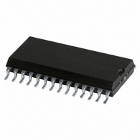
SJA1000T/N,118 NXP Semiconductors, SJA1000T/N,118 Datasheet - Page 49

SJA1000T/N,118
Manufacturer Part Number
SJA1000T/N,118
Description
IC STAND-ALONE CAN CTRLR 28-SOIC
Manufacturer
NXP Semiconductors
Datasheet
1.SJA1000TN1112.pdf
(68 pages)
Specifications of SJA1000T/N,118
Controller Type
CAN Interface
Interface
CAN
Voltage - Supply
4.5 V ~ 5.5 V
Current - Supply
15mA
Operating Temperature
-40°C ~ 125°C
Mounting Type
Surface Mount
Package / Case
28-SOIC (7.5mm Width)
Lead Free Status / RoHS Status
Lead free / RoHS Compliant
Other names
935277294118
SJA1000T/N-T
SJA1000T/N-T
SJA1000T/N-T
SJA1000T/N-T
Philips Semiconductors
6.4.16
The RMC register (CAN address 29) reflects the number of messages available within the RXFIFO. The value is
incremented with each receive event and decremented by the release receive buffer command. After any reset event,
this register is cleared.
Table 42 Bit interpretation of the RX message counter (RMC); CAN address 29
Note
1. This bit cannot be written. During read-out of this register always a zero is given.
6.4.17
The RBSA register (CAN address 30) reflects the currently
valid internal RAM address, where the first byte of the
received message, which is mapped to the receive buffer
window, is stored. With the help of this information it is
possible to interpret the internal RAM contents.
The internal RAM address area begins at CAN address 32
and may be accessed by the CPU for reading and writing
(writing in reset mode only).
Example: if RBSA is set to 24 (decimal), the current
message visible in the receive buffer window
(CAN address 16 to 28) is stored within the internal RAM
beginning at RAM address 24. Because the RAM is also
mapped directly to the CAN address space beginning at
CAN address 32 (equal to RAM address 0) this message
may also be accessed using CAN address 56 and the
following bytes
(CAN address = RBSA + 32 > 24 + 32 = 56).
Table 43 Bit interpretation of the RX buffer start address register (RBSA); CAN address 30
Note
1. This bit cannot be written. During read-out of this register always a zero is given.
2000 Jan 04
Stand-alone CAN controller
BIT 7
BIT 7
(0)
(0)
(1)
(1)
RX M
RX B
UFFER
ESSAGE
BIT 6
BIT 6
(0)
(0)
S
TART
(1)
(1)
C
OUNTER
A
DDRESS REGISTER
(RMC)
RBSA.5
BIT 5
BIT 5
(0)
(1)
(RBSA)
RBSA.4
RMC.4
BIT 4
BIT 4
49
If a message exceeds RAM address 63, it continues at
RAM address 0.
The release receive buffer command is always given while
there is at least one more message available within the
FIFO. RBSA is updated to the beginning of the next
message.
On hardware reset, this pointer is initialized to ‘00H’. Upon
a software reset (setting of reset mode) this pointer keeps
its old value, but the FIFO is cleared; this means that the
RAM contents are not changed, but the next received (or
transmitted) message will override the currently visible
message within the receive buffer window.
The RX buffer start address register appears to the CPU
as a read only memory in operating mode and as
read/write memory in reset mode. It should be noted that a
write access to RBSA takes effect first after the next
positive edge of the internal clock frequency, which is half
of the external oscillator frequency.
RBSA.3
RMC.3
BIT 3
BIT 3
RBSA.2
RMC.2
BIT 2
BIT 2
RBSA.1
RMC.1
BIT 1
BIT 1
Product specification
SJA1000
RBSA.0
RMC.0
BIT 0
BIT 0


