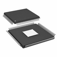
AD9910BSVZ Analog Devices Inc, AD9910BSVZ Datasheet - Page 11

AD9910BSVZ
Manufacturer Part Number
AD9910BSVZ
Description
IC DDS 1GSPS 14BIT PAR 100TQFP
Manufacturer
Analog Devices Inc
Datasheet
1.AD9910BSVZ-REEL.pdf
(64 pages)
Specifications of AD9910BSVZ
Design Resources
Synchronizing Multiple AD9910 1 GSPS Direct Digital Synthesizers (CN0121)
Resolution (bits)
14 b
Master Fclk
1GHz
Tuning Word Width (bits)
32 b
Voltage - Supply
1.8V, 3.3V
Operating Temperature
-40°C ~ 85°C
Mounting Type
Surface Mount
Package / Case
100-TQFP Exposed Pad, 100-eTQFP, 100-HTQFP, 100-VQFP
Pll Type
Frequency Synthesis
Frequency
1GHz
Supply Current
29mA
Supply Voltage Range
1.71V To 1.89V
Digital Ic Case Style
TQFP
No. Of Pins
100
Operating Temperature Range
-40°C To +85°C
Lead Free Status / RoHS Status
Lead free / RoHS Compliant
For Use With
AD9910/PCBZ - BOARD EVAL FOR AD9910 1GSPS
Lead Free Status / RoHS Status
Lead free / RoHS Compliant, Lead free / RoHS Compliant
Available stocks
Company
Part Number
Manufacturer
Quantity
Price
Company:
Part Number:
AD9910BSVZ
Manufacturer:
AVAGO
Quantity:
1 400
Company:
Part Number:
AD9910BSVZ
Manufacturer:
ADI
Quantity:
509
Company:
Part Number:
AD9910BSVZ
Manufacturer:
Analog Devices Inc
Quantity:
10 000
Part Number:
AD9910BSVZ
Manufacturer:
ADI/亚德诺
Quantity:
20 000
Company:
Part Number:
AD9910BSVZ-REEL
Manufacturer:
Analog Devices Inc
Quantity:
10 000
Table 3. Pin Function Descriptions
Pin No.
1, 20, 72, 86, 87,
93, 97 to 100
2
3, 6, 89, 92
74 to 77, 83
17, 23, 30, 47,
57, 64
11, 15, 21, 28, 45,
56, 66
4, 5, 73, 78, 79, 82,
85, 88, 96
13, 16, 22, 29, 46,
51, 58, 65
7
8
9
10
12
14
18
19
24
25 to 27, 31 to 39,
42 to 44, 48
49, 50
40
41
52 to 54
55
Mnemonic
NC
PLL_LOOP_FILTER
AVDD (1.8V)
AVDD (3.3V)
DVDD (1.8V)
DVDD_I/O (3.3V)
AGND
DGND
SYNC_IN+
SYNC_IN−
SYNC_OUT+
SYNC_OUT−
SYNC_SMP_ERR
MASTER_RESET
EXT_PWR_DWN
PLL_LOCK
RAM_SWP_OVR
D[15:0]
F[1:0]
PDCLK
TxENABLE
PROFILE[2:0]
SYNC_CLK
I/O
I
I
I
I
I
I
I
I
I
O
O
O
I
I
O
O
I
I
O
I
I
O
1
Description
Not Connected. Allow device pins to float.
PLL Loop Filter Compensation Pin. See the External PLL Loop Filter Components section for
details.
Analog Core VDD, 1.8 V Analog Supplies.
Analog DAC VDD, 3.3 V Analog Supplies.
Digital Core VDD, 1.8 V Digital Supplies.
Digital Input/Output VDD, 3.3 V Digital Supplies.
Analog Ground.
Digital Ground.
Synchronization Signal (LVDS), Digital Input (Rising Edge Active). The synchronization
signal from the external master to synchronize internal subclocks. See the Synchronization
of Multiple Devices section for details.
Synchronization Signal (LVDS), Digital Input. The synchronization signal from the external
master to synchronize internal subclocks. See the Synchronization of Multiple Devices
section for details.
Synchronization Signal (LVDS), Digital Output (Rising Edge Active). The synchronization
signal from the internal device subclocks to synchronize external slave devices. See the
Synchronization of Multiple Devices section for details.
Synchronization Signal (LVDS), Digital Output. The synchronization signal from the internal
device subclocks to synchronize external slave devices. See the Synchronization of Multiple
Devices section for details.
Synchronization Sample Error, Digital Output (Active High). Sync sample error: a high on
this pin indicates that the AD9910 did not receive a valid sync signal on SYNC_IN+/SYNC_IN−.
Master Reset, Digital Input (Active High). Master reset: clears all memory elements and sets
registers to default values.
External Power-Down, Digital Input (Active High). A high level on this pin initiates the
currently programmed power-down mode. See the Power-Down Control section for
further details. If unused, connect to ground.
Clock Multiplier PLL Lock, Digital Output (Active High). A high on this pin indicates that the
Clock Multiplier PLL has acquired lock to the reference clock input.
RAM Sweep Over, Digital Output (Active High). A high on this pin indicates that the RAM
sweep profile has completed.
Parallel Input Bus (Active High).
Modulation Format Pin. Digital input to determine the modulation format.
Parallel Data Clock. This is the digital output (clock). The parallel data clock provides a
timing signal for aligning data at the parallel inputs.
Transmit Enable. Digital input (active high). In burst mode communications, a high on this
pin indicates new data for transmission. In continuous mode, this pin remains high.
Profile Select Pins. Digital inputs (active high). Use these pins to select one of eight
phase/frequency profiles for the DDS. Changing the state of one of these pins transfers the
current contents of all I/O buffers to the corresponding registers. State changes should be
set up on the SYNC_CLK pin.
Output Clock Divided-By-Four. A digital output (clock). Many of the digital inputs on the
chip, such as I/O_UPDATE and PROFILE[2:0], need to be set up on the rising edge of this signal.
Rev. C | Page 11 of 64
AD9910


