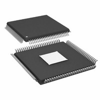
AD9910BSVZ Analog Devices Inc, AD9910BSVZ Datasheet - Page 27

AD9910BSVZ
Manufacturer Part Number
AD9910BSVZ
Description
IC DDS 1GSPS 14BIT PAR 100TQFP
Manufacturer
Analog Devices Inc
Datasheet
1.AD9910BSVZ-REEL.pdf
(64 pages)
Specifications of AD9910BSVZ
Design Resources
Synchronizing Multiple AD9910 1 GSPS Direct Digital Synthesizers (CN0121)
Resolution (bits)
14 b
Master Fclk
1GHz
Tuning Word Width (bits)
32 b
Voltage - Supply
1.8V, 3.3V
Operating Temperature
-40°C ~ 85°C
Mounting Type
Surface Mount
Package / Case
100-TQFP Exposed Pad, 100-eTQFP, 100-HTQFP, 100-VQFP
Pll Type
Frequency Synthesis
Frequency
1GHz
Supply Current
29mA
Supply Voltage Range
1.71V To 1.89V
Digital Ic Case Style
TQFP
No. Of Pins
100
Operating Temperature Range
-40°C To +85°C
Lead Free Status / RoHS Status
Lead free / RoHS Compliant
For Use With
AD9910/PCBZ - BOARD EVAL FOR AD9910 1GSPS
Lead Free Status / RoHS Status
Lead free / RoHS Compliant, Lead free / RoHS Compliant
Available stocks
Company
Part Number
Manufacturer
Quantity
Price
Company:
Part Number:
AD9910BSVZ
Manufacturer:
AVAGO
Quantity:
1 400
Company:
Part Number:
AD9910BSVZ
Manufacturer:
ADI
Quantity:
509
Company:
Part Number:
AD9910BSVZ
Manufacturer:
Analog Devices Inc
Quantity:
10 000
Part Number:
AD9910BSVZ
Manufacturer:
ADI/亚德诺
Quantity:
20 000
Company:
Part Number:
AD9910BSVZ-REEL
Manufacturer:
Analog Devices Inc
Quantity:
10 000
External PLL Loop Filter Components
The PLL_LOOP_FILTER pin provides a connection interface to
attach the external loop filter components. The ability to use
custom loop filter components gives the user more flexibility to
optimize the PLL performance. The PLL and external loop filter
components are shown in Figure 35.
In the prevailing literature, this configuration yields a third-
order, Type II PLL. To calculate the loop filter component
values, begin with the feedback divider value (N), the gain of
the phase detector (K
the programmed VCO SEL bit settings (see Table 1 for K
loop filter component values depend on the desired open-loop
bandwidth (f
where:
K
K
Ensure that proper units are used for the variables in Equation 4
through Equation 6. I
as appears in Table 9; K
megahertz per volts (MHz/V) as listed in Table 1; the loop
bandwidth (f
must be in radians.
For example, suppose the PLL is programmed such that I
287 μA, K
bandwidth and phase margin are 50 kHz and 45°, respectively,
then the loop filter component values are R1 = 52.85 Ω, C1 =
145.4 nF, and C2 = 30.11 nF.
D
V
is equal to the programmed value of I
is taken from Table 1.
C1 =
C2
R1
PLL IN
=
=
V
K
K
π
N
= 625 MHz/V, and N = 25. If the desired loop
2
Nf
D
D
K
(
OL
N
OL
2
K
K
Figure 35. REFCLK PLL External Loop Filter
OL
D
f π
) and phase margin (φ), as follows:
) must be in hertz (Hz); the phase margin (φ)
(
V
V
f π
K
OL
tan
⎛
⎜
⎜
⎝
V
OL
1
)
REFCLK PLL
+
)
2
( )
D
φ
2
⎛ −
⎜
⎜
⎝
CP
PFD
sin
), and the gain of the VCO (K
1
V
must be in amps, not microamps (μA)
cos
1
must be in hertz per volts (Hz/V), not
( )
φ
sin
( )
⎞
⎟
⎟
⎠
φ
( )
C1
÷N
CP
R1
φ
AVDD
⎞
⎟
⎟
⎠
2
PLL_LOOP_FILTER
C2
VCO
CP
.
PLL OUT
V
) based on
V
CP
). The
=
Rev. C | Page 27 of 64
(4)
(5)
(6)
PLL LOCK INDICATION
When the PLL is in use, the PLL_LOCK pin provides an active
high indication that the PLL has locked to the REFCLK input
signal. Note that the PLL_LOCK pin is a latched output. When the
PLL is bypassed, the pin may remain at Logic 1. The PLL_LOCK
pin can be cleared by setting the PFD reset bit. The PFD reset
bit must be cleared for normal operation.
OUTPUT SHIFT KEYING (OSK)
The OSK function (see Figure 36) allows the user to control the
output signal amplitude of the DDS. Both a manual and an
automatic mode are available under program control. The
amplitude data generated by the OSK block has priority over
any other functional block that is programmed to deliver
amplitude data to the DDS. Therefore, the OSK data source,
when enabled, overrides all other amplitude data sources.
The operation of the OSK function is governed by two CFR1
register bits (OSK enable and select auto OSK), the external
OSK pin, and the entire 32 bits of the ASF register. The primary
control for the OSK block is the OSK Enable bit. When the OSK
function is disabled, the OSK input controls are ignored and the
internal clocks shut down.
When the OSK function is enabled, automatic or manual
operation is selected using the select auto OSK bit. A Logic 0
indicates manual mode (default).
Manual OSK
In manual mode, output amplitude is varied by successive write
operations to the amplitude scale factor portion of the ASF
register. The rate at which amplitude changes can be applied to
the output signal is limited by the speed of the serial I/O port.
In manual mode, the OSK pin functionality depends on the
state of the manual OSK external control bit. When the OSK
pin is Logic 0, the output amplitude is forced to 0; otherwise,
the output amplitude is set by the amplitude scale factor value.
AMPLITUDE SCALE FACTOR
LOAD ARR AT I/O_UPDATE
AMPLITUDE RAMP RATE
AMPLITUDE STEP SIZE
MANUAL OSK EXTERNAL
(ASF[31:16])
(ASF[15:2])
AUTO OSK ENABLE
(ASF[1:0])
OSK ENABLE
Figure 36. OSK Block Diagram
16
14
2
CONTROLLER
DDS CLOCK
OSK
OSK
60
14
TO DDS
AMPLITUDE
CONTROL
PARAMETER
AD9910


