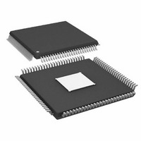
AD9910BSVZ Analog Devices Inc, AD9910BSVZ Datasheet - Page 46

AD9910BSVZ
Manufacturer Part Number
AD9910BSVZ
Description
IC DDS 1GSPS 14BIT PAR 100TQFP
Manufacturer
Analog Devices Inc
Datasheet
1.AD9910BSVZ-REEL.pdf
(64 pages)
Specifications of AD9910BSVZ
Design Resources
Synchronizing Multiple AD9910 1 GSPS Direct Digital Synthesizers (CN0121)
Resolution (bits)
14 b
Master Fclk
1GHz
Tuning Word Width (bits)
32 b
Voltage - Supply
1.8V, 3.3V
Operating Temperature
-40°C ~ 85°C
Mounting Type
Surface Mount
Package / Case
100-TQFP Exposed Pad, 100-eTQFP, 100-HTQFP, 100-VQFP
Pll Type
Frequency Synthesis
Frequency
1GHz
Supply Current
29mA
Supply Voltage Range
1.71V To 1.89V
Digital Ic Case Style
TQFP
No. Of Pins
100
Operating Temperature Range
-40°C To +85°C
Lead Free Status / RoHS Status
Lead free / RoHS Compliant
For Use With
AD9910/PCBZ - BOARD EVAL FOR AD9910 1GSPS
Lead Free Status / RoHS Status
Lead free / RoHS Compliant, Lead free / RoHS Compliant
Available stocks
Company
Part Number
Manufacturer
Quantity
Price
Company:
Part Number:
AD9910BSVZ
Manufacturer:
AVAGO
Quantity:
1 400
Company:
Part Number:
AD9910BSVZ
Manufacturer:
ADI
Quantity:
509
Company:
Part Number:
AD9910BSVZ
Manufacturer:
Analog Devices Inc
Quantity:
10 000
Part Number:
AD9910BSVZ
Manufacturer:
ADI/亚德诺
Quantity:
20 000
Company:
Part Number:
AD9910BSVZ-REEL
Manufacturer:
Analog Devices Inc
Quantity:
10 000
AD9910
(that is, they are synchronized). This concept is shown in Figure 53,
in which three AD9910 devices are synchronized, with one device
operating as a master timing unit and the others as slave units.
The master device must have its SYNC_INx pins included as part
of the synchronization distribution and delay equalization mec
nism in order for it to be synchronized with the slave units.
The synchronization mechanism begins with the clock distribu-
tion and delay equalization block, which is used to ensure that
all devices receive an edge-aligned REFCLK signal. However,
even though the REFCLK signal is edge aligned among all devices
this alone does not guarantee that the clock state of each internal
clock generator is coordinated with the others. This is the role
of the synchronization and delay equalization block. This block
accepts the SYNC_OUTx signal generated by the master device
and redistributes it to the SYNC_INx input of the slave units (as
well as feeding it back to the master). The goal of the redistribut
SYNC_OUT x signal from the master device is to deliver an
edge-aligned SYNC_INx signal to all of the sync receivers.
Assuming that all devices share the same REFCLK edge (due
the clock distribution and delay equalization block), and all
devices share the same SYNC_INx edge (due to the synchron
zation and delay equalization block), then all devices should
generate an internal sync pulse in unison (assuming that they
all have the same sync receiver delay value). With the further
stipulation that all devices have the same sync state preset valu
then the synchronized sync pulses cause all of the devices to
assume the same predefined clock state simultaneously; that is,
the internal clocks of all devices become fully synchronized.
RECEIVER
SYSCLK
DELAY
LOGIC
FROM
SYNC
SYNC TIMING VALIDATION DISABLE
DELAY
DELAY
Figure 54. Sync Timing Validation Block
SETUP AND HOLD VALIDATION
RISING EDGE
AND STROBE
GENERATOR
DETECTOR
4
4
SYNC RECEIVER
D Q
4
SYNC VALIDATION
DELAY
Rev. C | Page 46 of 64
ha-
ed
to
i-
VALIDATION
e,
D Q
VALIDATION
,
SETUP
PULSE
SYNC
D Q
HOLD
TO
CLOCK
GENERATION
LOGIC
The synchronization mechanism depends on the reliable gen-
eration of a sync pulse by the edge detection block in the sync
receiver. Generation of a valid sync pulse, however, requires
proper sampling of the rising edge of the delayed SYNC_INx signal
with the rising edge of the local SYSCLK. If the edge timing of
these signals fails to meet the setup or hold time requirements
of the internal latches in the edge detection circuitry, then the
proper generation of the sync pulse is in jeopardy. The setup
and hold validation block (see Figure 54) gives the user a means
to validate that proper edge timing exists between the two signals.
The setup and hold validation block can be disabled via the
sync timing validation disable bit in Control Function Register 2.
The validation block makes use of a user-specified time window
(programmable in increments of ~150 ps via the 4-bit sync
validation delay word in the multichip sync register). The setup
validation and hold validation circuits use latches identical to
those in the rising edge detector and strobe generator. The
programmable time window is used to skew the timing between
the rising edges of the local SYSCLK signal and the rising edges
of the delayed SYNC_INx signal. If either the hold or setup
validation circuits fail to detect a valid edge sample, the condition
is indicated externally via the SYNC_SMP_ERR pin (active high).
The user must choose a sync validation delay value that is a
reasonable fraction of the SYSCLK period. For example, if the
SYSCLK frequency is 1 GHz (1 ns period), then a reasonable
value is 1 or 2 (150 ps or 300 ps). Choosing too large a value can
cause the SYNC_SMP_ERR pin to generate false error signals.
Choosing too small a value may cause instability.
12
12
SYNC_SMP_ERR


