DS90C032TM/NOPB National Semiconductor, DS90C032TM/NOPB Datasheet
DS90C032TM/NOPB
Specifications of DS90C032TM/NOPB
*DS90C032TM/NOPB
DS90C032TM
Available stocks


Related parts for DS90C032TM/NOPB

DS90C032TM/NOPB Summary of contents
Page 1
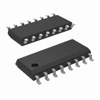
... Connection Diagrams Dual-In-Line Order Number DS90C032TM See NS Package Number M16A TRI-STATE ® registered trademark of National Semiconductor Corporation. © 2007 National Semiconductor Corporation Features ■ >155.5 Mbps (77.7 MHz) switching rates ■ Accepts small swing (350 mV) differential signal levels ■ ...
Page 2
Functional Diagram and Truth Tables Receiver EN L All other combinations of ENABLE inputs www.national.com 1194502 ENABLES INPUTS EN* R − ≥ V 0.1V ID ≤ V −0.1V ID Full Fail-safe OPEN/SHORT or Terminated 2 OUTPUT ...
Page 3
... Absolute Maximum Ratings If Military/Aerospace specified devices are required, please contact the National Semiconductor Sales Office/ Distributors for availability and specifications. Supply Voltage ( Input Voltage ( IN+ IN− Enable Input Voltage (EN, EN*) Output Voltage (R ) OUT Maximum Package Power Dissipation @ +25°C M Package E Package Derate M Package 8.2 mW/° ...
Page 4
Switching Characteristics V = +5.0V +25°C DS90C032T (Notes Symbol Parameter t Differential Propagation Delay High to Low PHLD t Differential Propagation Delay Low to High PLHD t Differential Skew |t − t ...
Page 5
Parameter Measurement Information FIGURE 1. Receiver Propagation Delay and Transition Time Test Circuit FIGURE 2. Receiver Propagation Delay and Transition Time Waveforms C includes load and test jig capacitance for t and t measurements ...
Page 6
Typical Application Applications Information LVDS drivers and receivers are intended to be primarily used in an uncomplicated point-to-point configuration as is shown in Figure 5. This configuration provides a clean signaling en- vironment for the quick edge rates of the ...
Page 7
The LVDS receiver is designed to detect very small amplitude and width signals and recover them to standard logic levels. ...
Page 8
Pin Descriptions Pin No. Name Description (SOIC 10, R Non-inverting receiver input pin IN Inverting receiver input pin IN− 11, R Receiver output pin OUT Active high ...
Page 9
Output Low Voltage vs Power Supply Voltage 1194510 Output Short Circuit Current vs Power Supply Voltage 1194512 Differential Propagation Delay vs Power Supply Voltage 1194514 Output Low Voltage vs Ambient Temperature Output Short Circuit Current vs Ambient Temperature Differential Propagation ...
Page 10
Differential Skew vs Power Supply Voltage Transition Time vs Power Supply Voltage www.national.com Differential Skew vs Ambient Temperature 1194516 Transition Time vs Ambient Temperature 1194518 10 1194517 1194519 ...
Page 11
Physical Dimensions inches (millimeters) unless otherwise noted 20-Lead Ceramic Leadless Chip Carrier, Type C 16-Lead (0.150 Wide) Molded Small Outline Package, JEDEC Order Number DS90C032E-QML NS Package Number E20A Order Number DS90C032TM NS Package Number M16A 11 www.national.com ...
Page 12
... National Semiconductor and the National Semiconductor logo are registered trademarks of National Semiconductor Corporation. All other brand or product names may be trademarks or registered trademarks of their respective holders. ...