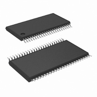
DS90C365AMT/NOPB National Semiconductor, DS90C365AMT/NOPB Datasheet - Page 10

DS90C365AMT/NOPB
Manufacturer Part Number
DS90C365AMT/NOPB
Description
IC XMITTER PROGR LVDS 48-TSSOP
Manufacturer
National Semiconductor
Type
Transmitterr
Datasheet
1.DS90C365AMTNOPB.pdf
(14 pages)
Specifications of DS90C365AMT/NOPB
Number Of Drivers/receivers
1/0
Protocol
RS644
Voltage - Supply
3 V ~ 3.6 V
Mounting Type
Surface Mount
Package / Case
48-TSSOP
Supply Current
60mA
Supply Voltage Range
3V To 3.6V
Driver Case Style
TSSOP
No. Of Pins
48
Operating Temperature Range
-10°C To +70°C
Msl
MSL 2 - 1 Year
Device Type
Clock
Termination Type
SMD
Rohs Compliant
Yes
Filter Terminals
SMD
Esd Hbm
7kV
Lead Free Status / RoHS Status
Lead free / RoHS Compliant
Other names
*DS90C365AMT/NOPB
DS90C365AMT
DS90C365AMT
www.national.com
TxIN
TxOUT+
TxOUT−
TxCLKIN
R_FB
TxCLK OUT+
TxCLK OUT−
PWR DOWN
V
GND
PLL V
PLL GND
LVDS V
LVDS GND
NC
CC
DS90C365A MTD48 (TSSOP) Package Pin Descriptions — FPD Link
Transmitter
Pin Name
CC
CC
I/O
O
O
O
O
I
I
I
I
I
I
I
I
I
I
No.
21
3
3
1
1
1
1
1
3
5
1
2
1
3
1
LVTTL level input. This includes: 6 Red, 6 Green, 6 Blue, and 3control lines—FPLINE, FPFRAME
and DRDY (also referred to as HSYNC, VSYNC, Data Enable).
Positive LVDS differentiaI data output.
Negative LVDS differential data output.
LVTTL Ievel clock input. Pin name TxCLK IN.
LVTTL Ievel programmable strobe select (See Table 1).
Positive LVDS differential clock output.
Negative LVDS differential clock output.
LVTTL level input. When asserted (low input) TRI-STATES the outputs, ensuring low current at
power down.
Power supply pins for LVTTL inputs.
Ground pins for LVTTL inputs.
Power supply pin for PLL.
Ground pins for PLL.
Power supply pin for LVDS outputs.
Ground pins for LVDS outputs.
No connect
10
Description


