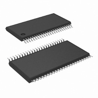
DS90C365AMT/NOPB National Semiconductor, DS90C365AMT/NOPB Datasheet

DS90C365AMT/NOPB
Specifications of DS90C365AMT/NOPB
DS90C365AMT
Related parts for DS90C365AMT/NOPB
DS90C365AMT/NOPB Summary of contents
Page 1
... FPDLink Receiver without any translation logic. This chipset is an ideal means to solve EMI and cable size problems associated with wide, high-speed TTL interfaces with added Spead Spectrum Clocking support.. Block Diagram © 2008 National Semiconductor Corporation Features ■ Pin-to-pin compatible to DS90C363, DS90C363A and DS90C365 . ...
Page 2
... Absolute Maximum Ratings If Military/Aerospace specified devices are required, please contact the National Semiconductor Sales Office/ Distributors for availability and specifications. Supply Voltage ( CMOS/TTL Input Voltage LVDS Driver Output Voltage LVDS Output Short Circuit Duration Junction Temperature Storage Temperature Lead Temperature (Soldering, 4 sec) Maximum Package Power Dissipation Capacity @ 25° ...
Page 3
Symbol Parameter ICCTG Transmitter Supply Current 16 Grayscale ICCTZ Transmitter Supply Current Power Down Note 1: “Absolute Maximum Ratings” are those values beyond which the safety of the device cannot be guaranteed. They are not meant to imply that the ...
Page 4
Transmitter Switching Characteristics Over recommended operating supply and temperature ranges unless otherwise specified Symbol LLHT LVDS Low-to-High Transition Time (Figure 4) LHLT LVDS High-to-Low Transition Time (Figure 4) TPPos0 Transmitter Output Pulse Position (Figure 12) (Note 5) TPPos1 Transmitter Output ...
Page 5
Symbol TCCD TxCLK IN to TxCLK OUT Delay. Measure from TxCLK IN edge to immediatley crossing poing of differential TxCLK OUT by following the postive TxCLK OUT. 50% duty cycle input clock is assumed. (Figure 7) Measure from TxCLK IN ...
Page 6
AC Timing Diagrams FIGURE 2. “16 Grayscale” Test Pattern - DS90C365A (Notes 8, 9, 10) Note 7: The worst case test pattern produces a maximum toggling of digital circuits, LVDS I/O and LVCMOS/LVTTL I/O. Note 8: The 16 grayscale test ...
Page 7
FIGURE 3. DS90C365A (Transmitter) LVDS Output Load. 5pF is showed as board loading FIGURE 4. DS90C365A (Transmitter) LVDS Transition Times FIGURE 5. DS90C365A (Transmitter) Input Clock Transition Time FIGURE 6. DS90C365A (Transmitter) Setup/Hold and High/Low Times with R_FB pin = ...
Page 8
FIGURE 8. DS90C365A (Transmitter) Clock In to Clock Out Delay with R_FB pin = GND FIGURE 9. DS90C365A (Transmitter) Phase Lock Loop Set Time FIGURE 10. 21 Parallel TTL Data Inputs Mapped to LVDS Outputs - DS90C365A www.national.com 20100535 20100514 ...
Page 9
FIGURE 11. Transmitter Power Down Delay FIGURE 12. Transmitter LVDS Output Pulse Position Measurement - DS90C365A 20100518 9 20100537 www.national.com ...
Page 10
DS90C365A MTD48 (TSSOP) Package Pin Descriptions — FPD Link Transmitter Pin Name I/O No. TxIN I 21 LVTTL level input. This includes: 6 Red, 6 Green, 6 Blue, and 3control lines—FPLINE, FPFRAME and DRDY (also referred to as HSYNC, VSYNC, ...
Page 11
Applications Information The DS90C365A is backward compatible DS90C365, DS90C363A, DS90C363 in TSSOP 48-lead package, and pin-for-pin replacements. This device DS90C365A also features reduced variation of the TCCD parameter which is important for dual pixel appli- cations. (See ...
Page 12
Typical Application Truth Table www.national.com TABLE 1. Programmable Transmitter (DS90C365A) Pin Condition Strobe Status R_FB R_FB = V Rising edge strobe CC R_FB R_FB = GND or NC Falling edge strobe 12 20100503 ...
Page 13
Physical Dimensions inches (millimeters) unless otherwise noted 48-Lead Molded Thin Shrink Small Outline Package, JEDEC Dimensions in millimeters only Order Number DS90C365AMT NS Package Number MTD48 13 www.national.com ...
Page 14
... For more National Semiconductor product information and proven design tools, visit the following Web sites at: Products Amplifiers www.national.com/amplifiers Audio www.national.com/audio Clock Conditioners www.national.com/timing Data Converters www.national.com/adc Displays www.national.com/displays Ethernet www.national.com/ethernet Interface www.national.com/interface LVDS www.national.com/lvds Power Management www.national.com/power Switching Regulators www.national.com/switchers LDOs www ...


