DS90CF364AMTD/NOPB National Semiconductor, DS90CF364AMTD/NOPB Datasheet
DS90CF364AMTD/NOPB
Specifications of DS90CF364AMTD/NOPB
*DS90CF364AMTD/NOPB
DS90CF364AMTD
Available stocks


Related parts for DS90CF364AMTD/NOPB

DS90CF364AMTD/NOPB Summary of contents
Page 1
... This chipset is an ideal means to solve EMI and cable size problems associated with wide, high speed TTL interfaces. Block Diagrams DS90CF384A Order Number DS90CF384AMTD See NS Package Number MTD56 TRI-STATE® registered trademark of National Semiconductor Corporation. © 2011 National Semiconductor Corporation DS90CF384A/DS90CF364A Features ■ MHz shift clock support ■ ...
Page 2
... Absolute Maximum Ratings If Military/Aerospace specified devices are required, please contact the National Semiconductor Sales Office/ Distributors for availability and specifications. Supply Voltage ( CMOS/TTL Input Voltage CMOS/TTL Output Voltage LVDS Receiver Input Voltage Junction Temperature Storage Temperature Lead Temperature (Soldering, 4 sec) Solder Reflow Temperature ...
Page 3
Note 1: “Absolute Maximum Ratings” are those values beyond which the safety of the device cannot be guaranteed. They are not meant to imply that the device should be operated at these limits. The tables of “Electrical Characteristics” specify conditions ...
Page 4
AC Timing Diagrams FIGURE 2. “16 Grayscale” Test Pattern www.national.com FIGURE 1. “Worst Case” Test Pattern (DS90CF384A)(Note 4 10087002 10087012 5, Note 6, Note 7, Note 8) ...
Page 5
FIGURE 3. “16 Grayscale” Test Pattern Note 5: The worst case test pattern produces a maximum toggling of digital circuits, LVDS I/O and CMOS/TTL I/O. Note 6: The 16 grayscale test pattern tests device power consumption for a “typical” LCD ...
Page 6
FIGURE 5. DS90CF384A/DS90CF364A (Receiver) Setup/Hold and High/Low Times FIGURE 6. DS90CF384A/DS90CF364A (Receiver) Clock In to Clock Out Delay FIGURE 7. DS90CF384A/DS90CF364A (Receiver) Phase Lock Loop Set Time www.national.com 10087005 10087006 6 10087007 ...
Page 7
FIGURE 8. 28 Parallel TTL Data Inputs Mapped to LVDS Outputs - DS90CF384A FIGURE 9. 21 Parallel TTL Data Inputs Mapped to LVDS Outputs - DS90CF364A FIGURE 10. DS90CF384A/DS90CF364A (Receiver) Power Down Delay 10087008 7 10087009 10087010 www.national.com ...
Page 8
FIGURE 11. DS90CF384A (Receiver) LVDS Input Strobe Position www.national.com 8 10087025 ...
Page 9
FIGURE 12. DS90CF364A (Receiver) LVDS Input Strobe Position 9 10087026 www.national.com ...
Page 10
C—Setup and Hold Time (Internal data sampling window) defined by Rspos (receiver input strobe position) min and max Tppos—Transmitter output pulse position (min and max) RSKM = Cable Skew (type, length) + Source Clock Jitter (cycle to cycle) + ISI ...
Page 11
DS90CF364A Pin Descriptions — 48L TSSOP Package — 18-Bit FPD Link Receiver Pin Name I/O No. RxIN Positive LVDS differentiaI data inputs. RxIN− Negative LVDS differential data inputs. RxOUT O 21 TTL level data outputs. This ...
Page 12
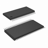
Physical Dimensions 56-Lead Molded Thin Shrink Small Outline Package, JEDEC 48-Lead Molded Thin Shrink Small Outline Package, JEDEC www.national.com inches (millimeters) unless otherwise noted Dimensions shown in millimeters only Order Number DS90CF384AMTD NS Package Number MTD56 Dimensions shown in millimeters ...
Page 13
Notes 13 www.national.com ...
Page 14
... For more National Semiconductor product information and proven design tools, visit the following Web sites at: www.national.com Products Amplifiers www.national.com/amplifiers Audio www.national.com/audio Clock and Timing www.national.com/timing Data Converters www.national.com/adc Interface www.national.com/interface LVDS www.national.com/lvds Power Management www.national.com/power Switching Regulators www.national.com/switchers LDOs www.national.com/ldo LED Lighting www ...